Series Roadmap
| # | Topic |
|---|---|
| 1 | The Origins of GPU and the Birth of SIMT — Tesla, Fermi |
| 2 | Kepler and Maxwell — The Pursuit of Efficiency |
| 3 | Pascal, Volta, Ampere — Toward Compute-Centric Design |
| 4 | GPU Memory Systems and Optimization |
| 5 | GPU Internals — Pipelines and Execution Units |
1. The Limits of Fermi — Where the Next Generation Began
Fermi (GF100, 2010) completed the GPU as a computing platform, introducing L1/L2 caches, ECC, and dual warp schedulers. But at 40nm, both performance and power efficiency had hit a ceiling.
Two problems demanded solutions.
The first was power consumption. GF100 packed 3 billion transistors onto a 529mm² die, drawing 250W TDP — too much for HPC clusters to manage per-rack.
The second was CPU-GPU coupling. Fermi had a single hardware work queue between CPU and GPU. In MPI environments, multiple CPU cores submitting GPU work were serialized through that one queue regardless.
NVIDIA addressed both over two successive generations, enabled by the move to 28nm.
2. Kepler — The Scale Experiment (2012)
SMX: Why 192 Cores?
The defining feature of Kepler (GK104/GK110, 2012) is 192 CUDA Cores per SM — a 6× increase from Fermi’s 32.
The reasoning is a clock-versus-count tradeoff. To reach a given throughput target with fewer cores running at higher frequency, the clocking logic itself burns more power. Kepler did the opposite: more cores at lower clock, yielding 3× performance-per-watt versus Fermi.
The SM was also renamed SMX (Streaming Multiprocessor eXtended).
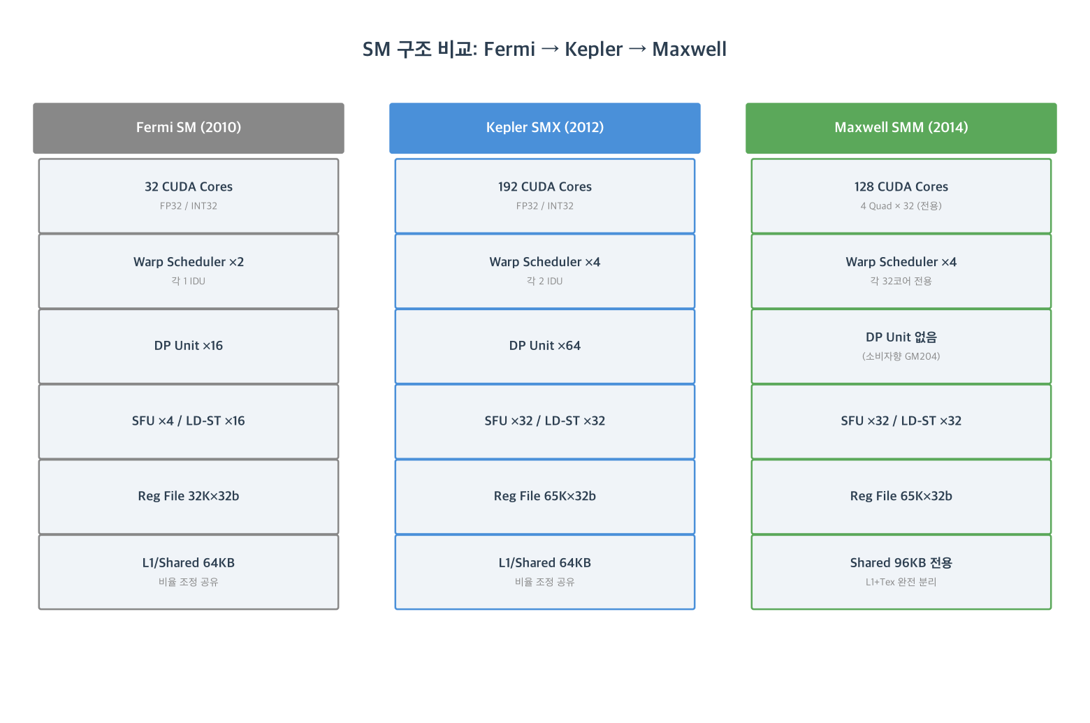
Fermi SM (GF100)           Kepler SMX (GK110)
────────────────            ──────────────────────────
 32 CUDA Cores               192 CUDA Cores
 Warp Sched ×2               Warp Sched ×4
  (1 IDU each)                (2 IDU each = 8 issues/clock)
 DP Unit ×16                 DP Unit ×64
 SFU ×4                      SFU ×32
 LD/ST ×16                   LD/ST ×32
 Reg File 32,768×32b=128KB   Reg File 65,536×32b=256KB
 L1+Shared 64KB (shared)     L1+Shared 64KB (shared)
 Max 48 warps/SM             Max 64 warps/SMX, 16 blocks/SMX
GK110 packed 15 SMX units for a total of 2,880 CUDA Cores.
4 Warp Schedulers and the ILP Dependency
Each SMX carries 4 warp schedulers, each with 2 IDUs — up to 8 instruction issues per clock.
One structural tension remains. The 192 cores are shared across 4 schedulers, giving 48 cores per scheduler — 16 more than a single warp. Filling that gap requires ILP (Instruction-Level Parallelism): issuing multiple independent instructions from the same warp simultaneously. Fermi could hide latency with thread-level parallelism (TLP) alone; Kepler requires kernel designs that expose ILP as well.
3. Kepler’s Software Innovations
Dynamic Parallelism
Before Kepler, each GPU kernel had to complete and return control to the CPU before the next kernel could be launched. For hierarchical computations — adaptive mesh refinement, tree traversal, sparse matrix operations — the CPU-GPU round-trip cost dominated.
Dynamic Parallelism, introduced in GK110 (Compute Capability 3.5), allows a kernel to launch child kernels from the GPU without CPU involvement.
Prior to Kepler                     Kepler Dynamic Parallelism
──────────────────────              ──────────────────────────────
CPU: launch kernel_A                CPU: launch kernel_A
GPU: execute kernel_A                  GPU: execute kernel_A
  return to CPU                             ↳ launch kernel_B (on GPU)
CPU: launch kernel_B                          GPU: execute kernel_B
GPU: execute kernel_B                               ↳ launch kernel_C ...
  return to CPU                      CPU: receive final result
...
Hyper-Q
Fermi provided a single hardware work queue between the host and GPU. In multi-process MPI jobs, all CPU cores funneled through that one connection, leaving GPU SMX units idle while the queue serialized work.
Hyper-Q expands this to 32 independent hardware-managed connections. Each MPI task, CUDA stream, or CPU thread can have its own queue, keeping the GPU’s SMX units fed from multiple sources simultaneously.
Fermi                       Kepler Hyper-Q
──────                      ────────────────────────
CPU Core 0 ─┐               CPU Core 0 ──→ [Queue 0]─┐
CPU Core 1 ─┤               CPU Core 1 ──→ [Queue 1] │
CPU Core 2 ─┼─→ [1 queue]   CPU Core 2 ──→ [Queue 2] ├──→ GPU
CPU Core 3 ─┤               ...                       │
...         ─┘               MPI Task N ──→ [Queue 31]┘
             ↓               (up to 32 simultaneous)
            GPU
Warp Shuffle
Sharing data between threads within a warp previously required Shared Memory: write → synchronize → read. Warp Shuffle instructions (__shfl_sync()), introduced at CC 3.0, allow direct register-to-register exchange within a warp — no Shared Memory involved.
// Warp-level reduction without Shared Memory
int val = threadIdx.x;
for (int offset = 16; offset > 0; offset >>= 1)
    val += __shfl_down_sync(0xffffffff, val, offset);
// Lane 0 holds the warp sum
4. Maxwell — Refinement over Scale (2014)
The Problem with 192-Core SMX
Kepler’s 48 cores per scheduler versus a warp width of 32 created a structural mismatch. Bridging that 16-core gap demanded ILP, adding pressure on both the compiler and the programmer.
Maxwell (GM107/GM204, 2014) answered with reduction and dedication.
SMM: The Quadrant Design
Maxwell SM is called SMM (Streaming Multiprocessor Maxwell). Core count drops to 128, but the SM is divided into 4 fully independent Quadrants.
Maxwell SMM (GM204, 128 CUDA Cores)
┌─────────────────────┬─────────────────────┐
│   Quadrant 0        │   Quadrant 1        │
│   Warp Scheduler    │   Warp Scheduler    │
│   32 CUDA Cores     │   32 CUDA Cores     │
│   (dedicated)       │   (dedicated)       │
├─────────────────────┼─────────────────────┤
│   Quadrant 2        │   Quadrant 3        │
│   Warp Scheduler    │   Warp Scheduler    │
│   32 CUDA Cores     │   32 CUDA Cores     │
│   (dedicated)       │   (dedicated)       │
└─────────────────────┴─────────────────────┘
         Shared Memory 96KB (dedicated)
         L1 Cache + Texture Cache (separate)
Each scheduler exclusively owns 32 cores — exactly one warp wide. A single-issue instruction fully utilizes all assigned cores. The ILP dependency that Kepler imposed is eliminated at the hardware level.
The numbers bear this out: 40% higher delivered performance per CUDA Core over Kepler, and 2× the overall SM efficiency of Kepler GK104 — achieved on the same 28nm process.
Dedicated Shared Memory
In Fermi and Kepler, L1 cache and Shared Memory competed for the same 64KB of on-chip storage. More L1 meant less Shared Memory and vice versa. Programmers set the ratio via cudaFuncSetCacheConfig() at kernel launch.
Maxwell separates them completely. Shared Memory gets dedicated on-chip storage (64KB on GM107, 96KB on GM204). L1 merges with the Texture Cache and operates independently.
Fermi / Kepler              Maxwell
──────────────              ─────────────────────
┌──────────────┐            ┌────────────────┐
│  64KB shared │            │ Shared Memory  │
│  ┌──┬──────┐ │            │ (64–96KB,      │
│  │L1│Shared│ │            │  dedicated)    │
│  │16│ 48KB │ │            └────────────────┘
│  └──┴──────┘ │            ┌────────────────┐
└──────────────┘            │ L1 + Tex Cache │
(or 48/16 ratio)            │   (separate)   │
                            └────────────────┘
L1 hit rate and Shared Memory utilization can now be maximized independently.
Compiler-Managed Register Reuse
Kepler relied on a runtime Operand Collector to resolve register bank conflicts on the fly. Maxwell replaces this with a compiler-managed Register Reuse Cache: the compiler schedules register reads so recently-used operands remain cached, eliminating bank conflicts statically. The dispatch path simplifies as a result.
CUDA Unified Memory (CUDA 6.0)
CUDA 6.0, released alongside Maxwell, introduced Unified Memory. Memory allocated via cudaMallocManaged() is accessible through a single pointer from both CPU and GPU; the runtime migrates pages automatically.
// Before: explicit separate allocations
float *h_data, *d_data;
h_data = (float*)malloc(size);
cudaMalloc(&d_data, size);
cudaMemcpy(d_data, h_data, size, cudaMemcpyHostToDevice);
kernel<<<grid, block>>>(d_data);
cudaMemcpy(h_data, d_data, size, cudaMemcpyDeviceToHost);

// Unified Memory: one pointer, automatic migration
float *data;
cudaMallocManaged(&data, size);
init_on_cpu(data);              // CPU initializes
kernel<<<grid, block>>>(data);  // GPU uses — migrated automatically
result = data[0];               // CPU reads result
The explicit cudaMemcpy() calls disappear. For performance-critical paths, explicit memory management is still advisable to avoid migration overhead.
5. Scheduling Evolution
Fermi SM               Kepler SMX             Maxwell SMM
──────────────         ──────────────         ──────────────
Sched A (1 IDU)        Sched A (2 IDU)        Quad 0: Sched
Sched B (1 IDU)        Sched B (2 IDU)          → 32 cores (own)
  ↓                    Sched C (2 IDU)        Quad 1: Sched
32 cores shared        Sched D (2 IDU)          → 32 cores (own)
                          ↓                   Quad 2: Sched
max 2 issues/clock     192 cores shared         → 32 cores (own)
TLP hides latency      max 8 issues/clock     Quad 3: Sched
                       TLP + ILP both needed    → 32 cores (own)
                                              single-issue = 100% util
                                              max blocks/SM: 32
                                              (Kepler: 16)
| Fermi | Kepler | Maxwell | |
|---|---|---|---|
| Warp Schedulers / SM | 2 | 4 | 4 |
| IDUs / Scheduler | 1 | 2 | 2 |
| Cores / Scheduler | 16 | 48 | 32 (= warp) |
| Latency hiding | TLP | TLP + ILP | TLP |
| Max Warps / SM | 48 | 64 | 64 |
| Max Blocks / SM | 8 | 16 | 32 |
| Shared Memory | shared with L1 | shared with L1 | dedicated |
Interconnect and External Channels
PCIe Host Interface
Kepler was NVIDIA’s first architecture with PCIe 3.0 x16 — 16 GB/s unidirectional, double PCIe 2.0. Maxwell retains PCIe 3.0 x16.
NVENC / NVDEC
| Kepler (GK104/GK110) | Maxwell (GM204/GM200) | |
|---|---|---|
| NVENC generation | 1st gen | 2nd gen |
| Encode codecs | H.264 | H.264 + HEVC |
| NVDEC generation | VP5 | VP6 |
| Decode codecs | H.264, VC-1 | + HEVC decode |
Kepler introduced the first hardware H.264 encoder (NVENC). Prior generations (Tesla, Fermi) had decode-only video units. Maxwell added HEVC (H.265) encode and decode.
Display Outputs (consumer reference cards)
| Product | DP | HDMI | DVI |
|---|---|---|---|
| GTX 680 (GK104) | 1.2 ×1 | 1.4 ×1 | ×2 |
| GTX 980 Ti (GM200) | 1.2 ×3 | 2.0 ×1 | ×1 |
Summary
| Kepler GK110 (2012) | Maxwell GM204 (2014) | |
|---|---|---|
| CUDA Cores / SM | 192 | 128 |
| SM internal structure | Monolithic | 4 Quadrants |
| Warp Schedulers / SM | 4 (2 IDU each) | 4 (32 dedicated cores each) |
| Cores / Scheduler | 48 | 32 |
| Register file / SM | 256 KB | 256 KB |
| L2 cache | GK110: 1.5 MB | GM204: 2 MB |
| DP Units / SM | 64 | — (consumer GM204) |
| Shared Memory | 64KB (shared with L1) | 96KB (dedicated) |
| PCIe | 3.0 x16 | 3.0 x16 |
| NVENC | 1st gen (H.264) | 2nd gen (H.264+HEVC) |
| Key features | Dynamic Parallelism, Hyper-Q, Warp Shuffle | Unified Memory, Quadrant design |
| Process | 28nm | 28nm |
| Representative products | Tesla K40, GTX 680 | GTX 980, GTX Titan X |
Kepler pursued throughput through scale. Maxwell doubled efficiency on the same process node through structural refinement.
The next post covers Pascal and Volta — HBM memory, NVLink, and the first Tensor Cores for deep learning acceleration.
References
- NVIDIA. NVIDIA’s Next Generation CUDA Compute Architecture: Kepler GK110/GK210 (Whitepaper, 2012). PDF
- NVIDIA. 5 Things You Should Know About the New Maxwell GPU Architecture. NVIDIA Developer Blog, 2014. Link
- NVIDIA. Maxwell: The Most Advanced CUDA GPU Ever Made. NVIDIA Developer Blog, 2014. Link
- NVIDIA. Maxwell Tuning Guide. CUDA Toolkit Documentation. Link
- NVIDIA. Tuning CUDA Applications for Kepler. CUDA Toolkit Documentation. Link
- Chester Lam. Maxwell: Nvidia’s Silver 28nm Hammer. Chips and Cheese, 2023. Link
한국어 버전은 상단 언어 스위처를 통해 확인할 수 있습니다.