Series Roadmap
| # | Topic | Status |
|---|---|---|
| 1 | Grace — NVIDIA’s First Datacenter CPU | ✅ |
| 2 | Vera / Rubin — GTC 2025 Announcement Summary | ✅ |
| 3 | (TBD) | 🔲 |
The PCIe Bottleneck
In a conventional server, the CPU and GPU communicate over PCIe. PCIe 5.0 x16 delivers approximately 64 GB/s of bandwidth — about 1/50th of an H100 SXM5’s HBM3 bandwidth (3.35 TB/s).
Getting data from CPU memory to the GPU requires an explicit copy:
Legacy PCIe:
[CPU DRAM] --cudaMemcpy--> [GPU DRAM] --compute--> [GPU DRAM] --cudaMemcpy--> [CPU DRAM]
               ~64 GB/s                                              ~64 GB/s
In LLM inference, token ingestion, KV cache management, and result return all pass through this bottleneck. Data movement — not GPU compute — becomes the limiting factor.
NVIDIA’s response was to design its own CPU. Grace is NVIDIA’s first datacenter CPU.
Core Architecture: Neoverse V2
Grace uses ARM’s Neoverse V2 (codename Demeter) microarchitecture — ARMv9.0-A ISA, 72 cores on a monolithic TSMC 4N die.
Instruction Scheduling and Execution Pipeline
Neoverse V2 is an out-of-order superscalar core. The frontend fetches and decodes instructions, renames registers, and dispatches to a unified reservation station. The backend issues instructions out-of-order to available execution units. A reorder buffer (ROB) commits results in program order.
Frontend                         Backend
┌─────────────┐                 ┌────────────────────────────────────┐
│ Fetch       │                 │     Unified Reservation Station    │
│ Decode      │────────────────>│                                    │
│ Rename      │                 │  INT ALU ×4   │  FP/SIMD/SVE2 ×2  │
│ Dispatch    │                 │  INT MUL ×2   │  Load/Store   ×2   │
└─────────────┘                 │  Branch   ×1  │                    │
                                └────────────┬───────────────────────┘
                                             │
                                    ┌────────▼────────┐
                                    │  ROB (in-order  │
                                    │  commit)        │
                                    └─────────────────┘
| Execution unit | Count |
|---|---|
| Integer ALU | 4 |
| Integer multiply | 2 |
| Branch | 1 |
| FP/SIMD/SVE2 | 2 |
| Load/store | 2 |
Branch prediction uses a multi-level TAGE predictor with a large history table to handle complex branch patterns.
SVE2 (Scalable Vector Extension 2) is implemented at 256-bit width in Grace. FP16, BF16, and INT8 — the precisions dominant in AI inference — are handled natively by the SVE2 pipelines, including BF16 accumulate instructions for CPU-side matrix operations.
Cache Hierarchy
The 72 cores are connected via an on-die mesh interconnect. Each core has private L1 and L2 caches; all cores share a large LLC.
[Core 0] [Core 1] [Core 2] ... [Core 11]
   │        │        │               │
  L2       L2       L2             L2
   │        │        │               │
   └────────┴────────┴───────────────┘
                     │
          [Shared L3 LLC (~114MB)]
                     │
          [LPDDR5X Memory Controller]
| Level | Size | Scope |
|---|---|---|
| L1 I-cache | 64 KB | Per core |
| L1 D-cache | 64 KB | Per core |
| L2 | 1 MB | Per core (private) |
| L3 (shared LLC) | ~114 MB | All 72 cores |
The 114 MB LLC is large by design — it keeps the working sets of multiple concurrent inference requests resident in cache, reducing DRAM access frequency.
Memory Subsystem: LPDDR5X
Datacenter CPUs conventionally use DDR5. Grace uses LPDDR5X — a standard originally designed for mobile devices, chosen for its high bandwidth-per-watt characteristics.
Grace delivers approximately 480 GB/s of memory bandwidth per die.
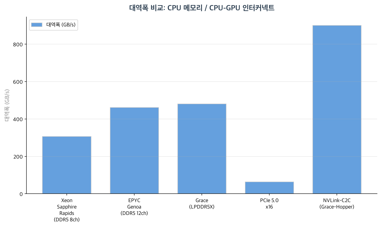
| CPU | Memory | Bandwidth |
|---|---|---|
| Intel Xeon Sapphire Rapids | DDR5-4800 8-ch | ~307 GB/s |
| AMD EPYC Genoa | DDR5-4800 12-ch | ~461 GB/s |
| NVIDIA Grace | LPDDR5X | ~480 GB/s |
| Grace CPU Superchip (2 dies) | LPDDR5X | ~960 GB/s |
LPDDR5X offers better bandwidth-per-watt than DDR5. Memory subsystem power is a significant share of total datacenter server power, making this metric relevant to total cost of ownership.
Each Grace die carries 96 GB of LPDDR5X. In a GH200, Grace’s 96 GB plus Hopper’s 80/96 GB HBM3 yields up to 192 GB of addressable memory in a single package.
Package Integration: Monolithic Die, Multi-Die Systems
Grace itself is a monolithic die — not a chiplet-based design like AMD EPYC’s CCD stack. All 72 cores reside on a single piece of silicon. NVIDIA packages this die in two configurations.
Grace CPU Superchip
Two Grace dies connected via NVLink-C2C — 144 cores in one package.
┌─────────────────────────────────────────────┐
│              Grace CPU Superchip            │
│  ┌───────────────┐       ┌───────────────┐  │
│  │  Grace Die 0  │       │  Grace Die 1  │  │
│  │  72 cores     │◄─────►│  72 cores     │  │
│  │  96 GB LPDDR5X│       │  96 GB LPDDR5X│  │
│  └───────────────┘       └───────────────┘  │
│            NVLink-C2C: 900 GB/s             │
└─────────────────────────────────────────────┘
           Total: 144 cores, 192 GB, ~960 GB/s
GH200 Grace-Hopper Superchip
One Grace CPU die and one Hopper GPU (H100 SXM5) on the same package — NVIDIA’s primary AI server building block.
┌──────────────────────────────────────────────────┐
│                  GH200 Superchip                 │
│  ┌────────────────┐          ┌─────────────────┐ │
│  │   Grace CPU    │          │   Hopper GPU    │ │
│  │   72 cores     │◄────────►│   H100 SXM5     │ │
│  │   96 GB LPDDR5X│          │   80/96 GB HBM3 │ │
│  └────────────────┘          └─────────────────┘ │
│           NVLink-C2C: 900 GB/s (bidirectional)   │
└──────────────────────────────────────────────────┘
NVLink-C2C
NVLink-C2C (Chip-to-Chip) is a NVLink variant specialized for intra-package die-to-die connections. It is distinct from the standard NVLink used to connect GPUs across a node (NVLink 4.0/5.0) — NVLink-C2C uses short-reach SerDes links on the package substrate.
| Property | NVLink-C2C | PCIe 5.0 x16 |
|---|---|---|
| Total bandwidth | 900 GB/s | ~64 GB/s |
| Unidirectional | 450 GB/s | ~32 GB/s |
| Cache coherency | Yes | No |
| Scope | Intra-package | System bus |
900 GB/s is ~14× PCIe 5.0 x16. While lower than GPU-to-GPU NVLink 5.0 (1,800 GB/s), NVLink-C2C’s critical differentiator is hardware cache coherency — absent from PCIe entirely.
NVL Rack-Scale Topology
Multiple GH200 nodes can be connected via NVLink Switch to form a single NVLink domain.
              NVLink Switch Fabric
       ┌──────────┬──────────┬──────────┐
       │          │          │          │
    GH200-0    GH200-1    GH200-2  ... GH200-31    (NVL32)
    ┌───────┐  ┌───────┐  ┌───────┐
    │Grace  │  │Grace  │  │Grace  │
    │+H100  │  │+H100  │  │+H100  │
    └───────┘  └───────┘  └───────┘
In an NVL32 configuration, all 32 GPUs can directly access each other’s HBM3 and each Grace CPU’s LPDDR5X. From a software perspective, this presents as one large shared address space across the rack. NCCL detects this topology automatically and routes collective operations along the highest-bandwidth paths.
GPU Connection and Command Architecture
Unified Virtual Address Space
NVLink-C2C’s hardware cache coherency means Grace and Hopper share a single virtual address space.
Legacy PCIe:
  CPU address space: [CPU DRAM 0x0000...]
  GPU address space: [GPU DRAM 0x0000...]  ← separate domains
  → Pointer sharing impossible. cudaMemcpy required.

GH200 NVLink-C2C:
  Unified address space: [Grace LPDDR5X | Hopper HBM3]
  → CPU ptr == GPU ptr. Pointers can be passed directly.
CUDA Programming Model Changes
| Operation | PCIe system | GH200 (NVLink-C2C) |
|---|---|---|
| CPU memory → GPU | cudaMemcpy required (~64 GB/s) |
GPU reads directly (~450 GB/s) |
| GPU result → CPU | cudaMemcpy required |
CPU reads directly |
cudaMallocManaged |
PCIe bandwidth ceiling | Full NVLink-C2C bandwidth |
| Pointer sharing | Impossible | Direct |
Memory allocated with cudaMallocManaged() is accessible from both CPU and GPU at full NVLink-C2C bandwidth — no staging buffers, no explicit copies. Code that previously required separate host and device allocations with explicit transfers can be simplified significantly.
What Hardware Cache Coherency Means in Practice
When the GPU reads a Grace LPDDR5X cache line that is currently in Grace’s L3, hardware coherency ensures the GPU sees the up-to-date value. When the GPU writes a cache line, Grace’s copy is automatically invalidated. The scope where software must issue explicit __threadfence_system() or cache flush calls is substantially narrowed compared to PCIe-based systems.
Software Support
| Component | Status |
|---|---|
| CUDA | Full support. cudaMallocManaged at full NVLink-C2C bandwidth |
| ARM SVE2 | GCC 11+, Clang 12+, Arm Compiler 22+ |
| OpenMP / OpenMPI | Full support |
| NCCL | Full support including multi-GH200 NVLink collectives |
| PyTorch / JAX / TensorFlow | Official ARM64 builds via PyPI |
| NVIDIA HPC SDK | Fortran/C/C++ with Neoverse V2 optimization, OpenACC GPU offload |
| OS | Ubuntu 22.04+, RHEL 9+ (ARM64) |
The NVIDIA HPC SDK supports SVE2 auto-vectorization and OpenACC GPU offload simultaneously — legacy Fortran/C HPC codes run on Grace without modification while still leveraging GPU acceleration.
Python packages for ARM64 are distributed via PyPI wheels, so pip install torch works on Grace without source builds.
Summary
| Item | Detail |
|---|---|
| Process | TSMC 4N |
| Cores | 72 × ARM Neoverse V2 (ARMv9.0-A) |
| SIMD | SVE2 256-bit |
| L3 cache | ~114 MB (shared across all 72 cores) |
| Memory | LPDDR5X, ~480 GB/s, 96 GB per die |
| On-die interconnect | Mesh NoC |
| GPU link | NVLink-C2C, 900 GB/s bidirectional, hardware cache coherency |
| Packaging | Grace CPU Superchip (2× Grace) or GH200 (Grace + H100) |
Grace is not designed to be a general-purpose high-performance CPU. Its goal is to eliminate the PCIe bottleneck and unify CPU and GPU into a single coherent compute domain. Neoverse V2 and LPDDR5X provide capable CPU-side compute and bandwidth; NVLink-C2C is what makes the unification real.