Series Roadmap
| # | Topic | Status |
|---|---|---|
| Overview | RDNA / CDNA Full Timeline | ✅ |
| 1 | RDNA 1 — Wave32, WGP, 7nm | ✅ |
| 2 | RDNA 2 — Ray Accelerator, Infinity Cache, Ampere comparison | ✅ |
| 3 | RDNA 3 — Chiplet (GCD+MCD), Dual-Issue shaders | 🔲 |
GCN’s Limitations
Before RDNA, every AMD GPU since 2011 ran on GCN (Graphics Core Next). GCN was modern for 2011 — a unified architecture handling both graphics and compute. After seven years of iteration without a fundamental redesign, structural problems had accumulated.
Two problems dominated.
1. Wave64 execution inefficiency
A GCN CU (Compute Unit) contained four SIMD16 units. The fundamental execution unit was a Wave64 — 64 threads in a wavefront. Each SIMD16 processed 16 threads per clock, so a Wave64 required 4 clocks to complete on one SIMD16.
The larger the wave, the worse divergence hurts. When only some of the 64 threads take an active branch, the rest stall. NVIDIA had already standardized on Warp32 (32-thread warps).
2. Low clock speeds
GCN was architected to hide memory latency through a large number of in-flight wavefronts rather than raw clock speed. Vega 64 boosted to roughly 1.5 GHz. Competing NVIDIA products ran well above 1.7 GHz.
RDNA 1 (Navi 10, 2019) addressed both problems simultaneously.
Wave32 and SIMD32: The Core Change
The most fundamental change in RDNA 1 is the execution width.
GCN CU:
┌─────────────────────────────────────────────────────┐
│  SIMD16[0]    SIMD16[1]    SIMD16[2]    SIMD16[3]  │
│  16 FP32      16 FP32      16 FP32      16 FP32     │
│                                                      │
│  ← Wave64: 64 threads / 4 clocks (SIMD16 × 4)      │
│    Each SIMD16 processes a separate wavefront        │
└──────────────────────────────────────────────────────┘
  64 FP32 ALUs per CU

RDNA 1 CU:
┌───────────────────────────────────────┐
│       SIMD32[0]       SIMD32[1]       │
│       32 FP32         32 FP32         │
│                                       │
│  ← Wave32: 32 threads / 1 clock      │
│    Each SIMD32 processes one wavefront│
└───────────────────────────────────────┘
  64 FP32 ALUs per CU (same count)
The FP32 ALU count per CU remains 64. What changed is the wave granularity.
What Wave32 Changes in Practice
| Property | GCN Wave64 | RDNA Wave32 |
|---|---|---|
| Thread count | 64 | 32 |
| SIMD width | 16 | 32 |
| Clocks to complete wave | 4 (16×4) | 1 (32×1) |
| Max divergence waste | 63/64 lanes idle | 31/32 lanes idle |
| NVIDIA compatibility | Different from Warp32 | Same width as Warp32 |
With Wave32, the worst-case divergence penalty is halved — at most 31 lanes wasted instead of 63. Because a wave completes in a single clock, fewer in-flight waves are needed to hide latency, which allows higher clock frequencies.
RDNA 1 also supports Wave64 (for GCN compatibility). In that mode, the two SIMD32s cooperate to handle 64 threads over 2 clocks.
WGP: A New Layer Above the CU
RDNA 1 introduced the WGP (Work Group Processor) — pairing two CUs together under a shared cache and shared scalar resources.
RDNA 1 WGP:
┌──────────────────────────────────────────────────────┐
│                        WGP                           │
│  ┌──────────────────────┐  ┌──────────────────────┐  │
│  │        CU [0]        │  │        CU [1]        │  │
│  │  SIMD32 × 2 (64 SP)  │  │  SIMD32 × 2 (64 SP)  │  │
│  │  LDS 32 KB           │  │  LDS 32 KB           │  │
│  │  Scalar Unit         │  │  Scalar Unit         │  │
│  └──────────┬───────────┘  └───────────┬──────────┘  │
│             └──────────┬───────────────┘              │
│               ┌────────▼─────────┐                   │
│               │  L0 vector cache │  (shared, 128 KB) │
│               │  Scalar cache    │  (shared,  32 KB) │
│               └──────────────────┘                   │
└──────────────────────────────────────────────────────┘
  WGP total: 4 × SIMD32 = 128 FP32 SPs
In GCN, each CU had a private 16 KB L1 cache. In RDNA 1, two CUs share a 128 KB L0 cache. When both CUs in a WGP access the same data, it hits the shared L0 instead of going to the next level.
Cache Hierarchy Redesign
RDNA 1 introduced a new intermediate cache level that GCN lacked entirely.
GCN (Vega 64):
CU → [L1 16 KB (per-CU, private)] → [L2 4 MB (global)] → HBM/GDDR

RDNA 1 (Navi 10):
CU → [L0 128 KB (per-WGP, 2-CU shared)]
   → [GL1 128 KB (per Shader Array)]
   → [L2 4 MB (global)] → GDDR6
The new GL1 (Global Level 1) cache sits between the WGP-level L0 and the chip-wide L2. All WGPs within a Shader Array share the GL1. Cache misses that previously went straight from L1 to L2 now have an intermediate stop.
| Level | GCN (Vega) | RDNA 1 (Navi 10) | Scope |
|---|---|---|---|
| Per-CU private | 16 KB | — | Per CU |
| WGP shared (L0) | None | 128 KB | Per WGP (2 CUs) |
| GL1 | None | 128 KB | Per Shader Array |
| L2 | 4 MB | 4 MB | Chip-wide |
Navi 10 Die Structure
Navi 10: TSMC 7nm, 251 mm², 10.3 billion transistors.
Navi 10 die:
┌────────────────────────────────────────────────────────┐
│                                                        │
│  ┌──────────┐  ┌──────────┐  ┌──────────┐  ┌────────┐ │
│  │  SE 0    │  │  SE 1    │  │  SE 2    │  │  SE 3  │ │
│  │ SA0│SA1  │  │ SA0│SA1  │  │ SA0│SA1  │  │SA0│SA1 │ │
│  │5WGP│5WGP │  │5WGP│5WGP │  │5WGP│5WGP │  │5WGP│5WGP│ │
│  │(GL1 128K)│  │          │  │          │  │        │ │
│  └──────────┘  └──────────┘  └──────────┘  └────────┘ │
│                                                        │
│  ┌──────────────────────────────────────────────────┐  │
│  │  L2 cache 4 MB (16 channels × 256 KB)            │  │
│  └──────────────────────────────────────────────────┘  │
│                                                        │
│  [GDDR6 MC × 8]  [Display Engine]  [Geometry Eng. × 4]│
└────────────────────────────────────────────────────────┘

SE: Shader Engine (4 total)
SA: Shader Array (2 per SE)
WGP: 5 per SA → 10 per SE → 40 WGPs total (20 CU pairs = 40 CUs)
RX 5700 XT uses all 40 CUs
RX 5700 XT specifications:
| Item | Value |
|---|---|
| Process | TSMC 7nm |
| Die area | 251 mm² |
| Transistors | 10.3 billion |
| CUs | 40 (20 WGPs) |
| Shader processors | 2,560 |
| ROPs | 64 |
| L2 cache | 4 MB |
| Memory | GDDR6 8 GB, 256-bit |
| Memory bandwidth | 448 GB/s |
| Boost clock | ~1905 MHz |
| FP32 throughput | 9.75 TFLOPS |
| TDP | 225 W |
| Interface | PCIe 4.0 x16 (first consumer GPU) |
The 1905 MHz boost clock is ~23% higher than Vega 64 (~1546 MHz) — a direct result of Wave32 requiring fewer in-flight waves to hide latency, combined with the power efficiency gain from 7nm.
Structural Comparison with NVIDIA Turing
The direct competitor to RDNA 1 was NVIDIA’s Turing architecture (RTX 20 series), launched September 2018 on TU102/TU104/TU106.
SM vs CU/WGP Execution Units
NVIDIA Turing SM (TU104):
┌──────────────────────────────────────────────────────┐
│                   Turing SM                          │
│  ┌───────────────────────────────────────────────┐   │
│  │  Warp Scheduler × 4   │  Dispatch Unit × 4   │   │
│  └───────────────────────────────────────────────┘   │
│  ┌────────┐ ┌────────┐ ┌────────┐ ┌────────┐         │
│  │FP32 ×16│ │FP32 ×16│ │FP32 ×16│ │FP32 ×16│         │
│  │INT32×16│ │INT32×16│ │INT32×16│ │INT32×16│         │
│  └────────┘ └────────┘ └────────┘ └────────┘         │
│  FP32: 64     INT32: 64   (FP32 + INT32 co-issue)   │
│  Tensor Core × 8     RT Core × 1                    │
│  Shared mem / L1: up to 96 KB                        │
└──────────────────────────────────────────────────────┘

AMD RDNA 1 WGP:
┌──────────────────────────────────────────────────────┐
│                   WGP                                │
│  ┌───────────────────────┐ ┌────────────────────┐   │
│  │       CU [0]          │ │       CU [1]       │   │
│  │  SIMD32 × 2 (64 SP)   │ │  SIMD32 × 2 (64 SP)│   │
│  │  (FP32 and INT32      │ │                    │   │
│  │   share the same ALUs)│ │                    │   │
│  └───────────────────────┘ └────────────────────┘   │
│  FP32: 128    INT32: shared with FP32, no co-issue  │
│  No Tensor Core    No RT Core                        │
│  L0 cache 128 KB (shared)                           │
└──────────────────────────────────────────────────────┘
Key Design Differences
1. FP32 + INT32 Dual Issue (Turing exclusive)
Turing SM has separate FP32 and INT32 pipelines. They can issue instructions simultaneously in the same clock — address computations (INT32) run while data operations (FP32) execute in parallel.
In RDNA 1, the FP32 ALUs also handle integer operations. FP32 and INT32 are not co-issuable; address calculation serializes with data computation.
2. Ray Tracing
Turing RT Cores accelerate BVH traversal and ray-box intersection tests in dedicated fixed-function hardware. DirectX Ray Tracing (DXR) is natively accelerated.
RDNA 1 has no RT hardware. DXR is technically supported through shader-based software fallback, but performance is impractical for real-time use.
3. Tensor Cores (AI acceleration)
Turing 2nd-gen Tensor Cores accelerate FP16, INT8, and INT4 matrix operations. DLSS 1.0 uses them for neural-network-based upscaling.
RDNA 1 has no matrix acceleration units. No equivalent to DLSS exists.
4. Independent Thread Scheduling
Starting with Volta, each NVIDIA thread has its own program counter and call stack, enabling reconvergence at sub-warp granularity.
RDNA 1 uses wavefront-level scheduling. Divergence within a wave is handled via an active-lane bitmask.
5. Process Node Gap
| RDNA 1 (Navi 10) | Turing (TU104) | |
|---|---|---|
| Process | TSMC 7nm | TSMC 12nm |
| Die area | 251 mm² | 545 mm² |
| Transistors | 10.3 B | 13.6 B |
| Transistor density | ~41 M/mm² | ~25 M/mm² |
RDNA 1 achieves comparable transistor counts in 54% of the die area. This directly translates to manufacturing cost and power envelope.
Specification Comparison (Direct Competition)
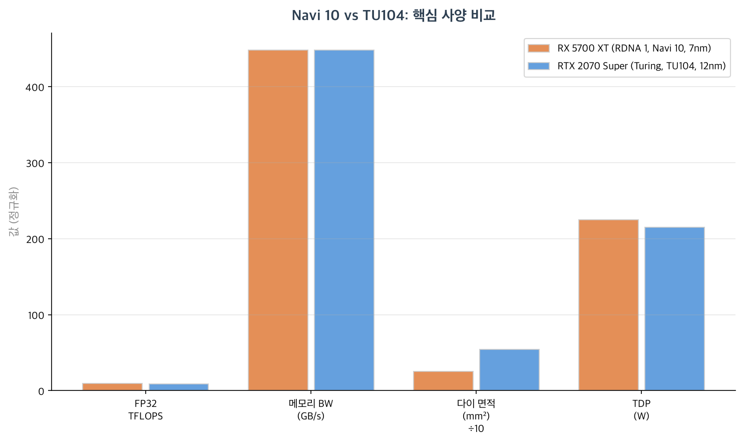
| RX 5700 XT (RDNA 1) | RTX 2070 Super (Turing) | RTX 2080 Super (Turing) | |
|---|---|---|---|
| Process | 7nm | 12nm | 12nm |
| Die | Navi 10 (251 mm²) | TU104 (545 mm²) | TU104 (545 mm²) |
| Shader count | 2,560 SP | 2,560 CUDA | 3,072 CUDA |
| FP32 TFLOPS | 9.75 | ~9.06 | ~11.1 |
| Memory BW | 448 GB/s | 448 GB/s | 496 GB/s |
| Ray tracing | None | 1st-gen RT Core | 1st-gen RT Core |
| Tensor / DLSS | None | 2nd-gen Tensor | 2nd-gen Tensor |
| PCIe | 4.0 | 3.0 | 3.0 |
| TDP | 225 W | 215 W | 250 W |
| Launch price | $399 | $499 | $699 |
In pure rasterization, the RX 5700 XT matched the RTX 2070 Super at $100 less. The 7nm process and Wave32 efficiency gains made this possible. Exclude ray tracing and DLSS, and RDNA 1 was competitive. Include them, and Turing had a feature tier RDNA 1 couldn’t match.
Software Stack: ROCm vs CUDA
The hardware gap was mirrored by the software ecosystem.
NVIDIA CUDA: 12+ years of compounding investment. cuBLAS, cuDNN, NCCL, TensorRT — every major ML framework targets CUDA first.
AMD ROCm: During the RDNA 1 era, ROCm support for RDNA-class hardware was limited. Formal compute support for RDNA GPUs improved in subsequent generations. For compute workloads in 2019–2020, Vega-based cards remained the ROCm-recommended option. RDNA 1 was primarily positioned as a gaming architecture, not a compute platform.
What RDNA 1 Achieved and What It Didn’t
Achieved:
- Wave32 as the native execution unit — divergence reduced, higher clocks enabled
- 7nm process: TU104-comparable rasterization in 54% of the die area
- WGP + expanded cache hierarchy: lower memory access latency
- PCIe 4.0 — first consumer GPU to do so
Not addressed:
- No dedicated RT hardware — addressed in RDNA 2
- No INT32 dedicated pipeline — Turing co-issue advantage remains
- No matrix acceleration — remains CDNA’s domain
- No DLSS-equivalent — FSR (software) came later, FSR 4 (AI-accelerated) not until RDNA 4
Summary
| Item | RDNA 1 (Navi 10) | vs GCN (Vega) | vs Turing (TU104) |
|---|---|---|---|
| Wave size | Wave32 | Half (64→32) | Same (Warp32) |
| SIMD width | 32 | 2× (16→32) | Same |
| Boost clock | ~1905 MHz | +23% | Comparable |
| Process | 7nm | Same | 5nm ahead |
| Die area | 251 mm² | — | 54% of TU104 |
| Ray tracing | None | None | Behind (Turing HW) |
| INT32 co-issue | None | None | Behind (Turing HW) |
| Tensor/matrix | None | None | Behind (Turing HW) |
| Rasterization perf/W | Improved | 1.25× (AMD claim) | Comparable |
RDNA 1 successfully broke from GCN. Wave32, WGP, and cache redesign improved execution efficiency and enabled higher clocks. But Turing’s RT Cores, Tensor Cores, and INT32 co-issue established a feature gap that rasterization efficiency alone couldn’t close. Closing that gap was left to RDNA 2.
Next: RDNA 2 — Ray Accelerator, Infinity Cache, and Big Navi