In 2019, AMD split its GPU architecture into two independent lines. RDNA targets consumer graphics; CDNA targets datacenter compute. This ended the era of GCN (Graphics Core Next, 2011–2019), where a single architecture handled both graphics and compute.
Full Timeline
Year  | RDNA (Consumer)                | CDNA (Datacenter)
------|--------------------------------|--------------------------
2019  | RDNA 1 — Navi 10, RX 5700     |
2020  | RDNA 2 — Navi 21, RX 6000     | CDNA 1 — Arcturus, MI100
2021  |                                | CDNA 2 — Aldebaran, MI200
2022  | RDNA 3 — Navi 31, RX 7000     |
2023  |                                | CDNA 3 — Aqua Vanjaram, MI300
2024  |                                | CDNA 3 — MI325X (HBM3e)
2025  | RDNA 4 — Navi 48, RX 9000     | CDNA 4 — MI350 (announced)
RDNA 1 (2019) — Navi 10
| Launch: July 2019 | Process: TSMC 7nm | Flagship: RX 5700 XT |
GCN’s core problem was its cache hierarchy. CUs did not share L1 cache, making inter-thread data sharing expensive.
RDNA 1 introduced the WGP (Work Group Processor) — two CUs paired together sharing a 128 KB L1 cache.
GCN                              RDNA 1
┌──┐ ┌──┐ ┌──┐ ┌──┐             ┌────────────┐ ┌────────────┐
│CU│ │CU│ │CU│ │CU│             │    WGP     │ │    WGP     │
│L1│ │L1│ │L1│ │L1│             │ CU0 | CU1 │ │ CU0 | CU1 │
└──┘ └──┘ └──┘ └──┘             │  L1 128KB  │ │  L1 128KB  │
Per-CU private L1, no sharing   └────────────┘ └────────────┘
Key features:
- First consumer GPU with PCIe 4.0
- 4 MB L2 per shader engine
- RX 5700 XT: 40 CUs, 2560 SPs, GDDR6 8 GB 256-bit
RDNA 2 (2020) — Navi 21
| Launch: November 2020 | Process: TSMC 7nm | Flagship: RX 6900 XT |
RDNA 2’s two headline additions were hardware ray tracing and Infinity Cache.
Ray Accelerator
The first hardware ray tracing unit in a consumer AMD GPU — one per CU. Handles BVH traversal and box-intersection tests in fixed-function hardware.
Infinity Cache
128 MB of on-die L3 cache (Navi 21). Its purpose is to reduce pressure on the external GDDR6 bus.
GDDR6 raw bandwidth:    512 GB/s  (256-bit × 16 Gbps)
Infinity Cache eff. BW: ~1,664 GB/s  (local reads on cache hit)
→ Effective bandwidth scales with hit rate — up to 3× at high locality
Infinity Cache compensated for GDDR6’s bandwidth limitations, delivering effective bandwidth competitive with HBM2-equipped competitors.
Key features:
- DirectX 12 Ultimate (Mesh Shaders, VRS, Sampler Feedback)
- Smart Access Memory (SAM): Resizable BAR, CPU addresses full GPU VRAM
- Xbox Series X and PlayStation 5 SoCs are based on RDNA 2
- RX 6900 XT: 80 CUs, 5120 SPs, 128 MB Infinity Cache, 16 GB GDDR6
CDNA 1 (2020) — Arcturus, MI100
| Launch: November 2020 | Process: TSMC 7nm | Product: Instinct MI100 |
CDNA 1 removed the graphics pipeline from GCN entirely, producing a pure-compute architecture.
Matrix Core
Matrix Core is the CDNA 1 compute accelerator — AMD’s counterpart to NVIDIA’s Tensor Core. It accelerates INT8, INT4, BF16, and FP16 matrix operations in dedicated fixed-function hardware.
CDNA 1 CU layout:
┌──────────────────────────────────────┐
│  4 × SIMD32 (FP32/FP64 vector ops)  │
│  4 × Matrix Core (INT8/BF16 matrix) │
│  LDS (Local Data Share)             │
└──────────────────────────────────────┘
Key features:
- No graphics pipeline or display output
- FP64 vector: 11.5 TFLOPS
- BF16 Matrix (Matrix Core): 184.6 TFLOPS
- HBM2: 32 GB, 1.23 TB/s
- Infinity Fabric 2.0 for inter-node connectivity
CDNA 2 (2021) — Aldebaran, MI200
| Launch: November 2021 | Process: TSMC N6 (6nm) | Product: Instinct MI250X |
CDNA 2 introduced AMD’s first GPU MCM (Multi-Chip Module) design — two GPU dies on a single OAM package.
MI250X OAM Package:
┌──────────────────────────────────────┐
│  ┌─────────────┐   ┌─────────────┐  │
│  │  GCD Die 0  │◄─►│  GCD Die 1  │  │
│  │  110 CUs    │   │  110 CUs    │  │
│  │  HBM2e ×2   │   │  HBM2e ×2   │  │
│  └─────────────┘   └─────────────┘  │
│     Infinity Fabric (inter-die)      │
└──────────────────────────────────────┘
       Total: 220 CUs, 128 GB HBM2e
Key features:
- 2-die MCM: 110 CUs per die, 220 CUs total
- HBM2e: 128 GB total, 3.2 TB/s total bandwidth
- FP64 Matrix Core added — CDNA 1 supported FP64 vector only
- FP64 vector: 47.9 TFLOPS, FP64 matrix: 95.7 TFLOPS, BF16: 383 TFLOPS
- Frontier supercomputer: MI250X-based first exascale system (June 2022, Top500 #1)
RDNA 3 (2022) — Navi 31
| Launch: December 2022 | Process: GCD 5nm / MCD 6nm | Flagship: RX 7900 XTX |
RDNA 3 is AMD’s first chiplet-based consumer GPU. The die is split by function.
Navi 31 Package:
┌──────────────────────────────────────────────────────────┐
│                                                          │
│  ┌────────────────────────────────────────────────────┐  │
│  │       GCD (Graphics Compute Die, 5nm)              │  │
│  │   12 Shader Engines × 8 WGPs × 2 CUs = 96 CUs     │  │
│  └────────────────────────────────────────────────────┘  │
│                                                          │
│  ┌──────┐ ┌──────┐ ┌──────┐ ┌──────┐ ┌──────┐ ┌──────┐ │
│  │MCD 0 │ │MCD 1 │ │MCD 2 │ │MCD 3 │ │MCD 4 │ │MCD 5 │ │
│  │16MB  │ │16MB  │ │16MB  │ │16MB  │ │16MB  │ │16MB  │ │
│  │IC    │ │IC    │ │IC    │ │IC    │ │IC    │ │IC    │ │
│  │MC64b │ │MC64b │ │MC64b │ │MC64b │ │MC64b │ │MC64b │ │
│  └──────┘ └──────┘ └──────┘ └──────┘ └──────┘ └──────┘ │
│              Infinity Fabric (GCD ↔ each MCD)            │
└──────────────────────────────────────────────────────────┘
- GCD: All shader compute, Ray Accelerators, geometry engines — 5nm for high yield on compute-intensive silicon
- MCD (Memory Cache Die): 16 MB Infinity Cache + 64-bit memory controller each; 6 MCDs = 96 MB IC + 384-bit bus — on cheaper 6nm
Key features:
- Dual-Issue shaders: each SIMD32 issues two instructions per clock (simple + complex pairing)
- 2nd-gen Ray Accelerators
- 2nd-gen AI Accelerators
- DisplayPort 2.1, AV1 hardware encode
- RX 7900 XTX: 96 CUs, 6144 SPs, 96 MB Infinity Cache, 24 GB GDDR6
CDNA 3 (2023) — Aqua Vanjaram, MI300 Series
| Launch: December 2023 | Process: XCD 5nm / IOD 6nm | Products: Instinct MI300X, MI300A |
CDNA 3’s defining feature is integrating CPU dies, GPU dies, and HBM into a single package.
MI300X: Pure GPU Configuration
Eight XCDs (eXelerate Compute Dies) plus four IODs (I/O Dies).
MI300X OAM Package:
┌──────────────────────────────────────────────────┐
│  XCD XCD XCD XCD    HBM3 HBM3 HBM3 HBM3         │
│  ─── ─── ─── ───    ─── ─── ─── ───             │
│       IOD  IOD                                   │
│       IOD  IOD                                   │
│  ─── ─── ─── ───    ─── ─── ─── ───             │
│  XCD XCD XCD XCD    HBM3 HBM3 HBM3 HBM3         │
└──────────────────────────────────────────────────┘
    8 XCDs × ~38 CUs = ~304 active CUs
    8 HBM3 stacks = 192 GB, 5.3 TB/s
MI300A: CPU+GPU HPC APU
Three GPU XCDs and three CPU CCDs (Zen 4) on the same package — the first datacenter APU to use unified HBM.
MI300A Package:
┌─────────────────────────────────────────────────┐
│  GPU XCD × 3   │  CPU CCD (Zen 4) × 3          │
│         HBM3 × 8 stacks (128 GB, 5.3 TB/s)     │
└─────────────────────────────────────────────────┘
CPU and GPU share the same HBM3 pool — no data copies required between CPU-computed results and GPU kernels.
Key features (MI300X):
- FP8: ~1307 TFLOPS, BF16: 1307 TFLOPS, FP64 vector: ~163 TFLOPS
- HBM3: 192 GB, 5.3 TB/s
- El Capitan supercomputer: MI300A-based, Top500 #1 as of 2024 (>2 EFlop/s)
MI325X (2024) — Memory Refresh
Same CDNA 3 architecture; HBM3 upgraded to HBM3e.
| Item | MI300X | MI325X |
|---|---|---|
| Architecture | CDNA 3 | CDNA 3 |
| GPU memory | HBM3 192 GB | HBM3e 288 GB |
| Memory bandwidth | 5.3 TB/s | 6.0 TB/s |
288 GB at 6.0 TB/s extends KV cache capacity directly for long-context LLM inference.
RDNA 4 (2025) — Navi 48
| Launch: March 2025 | Process: TSMC 4nm (N4P) | Flagship: RX 9070 XT |
RDNA 4 targets the performance tier without a high-end flagship. The Navi 48 die powers the RX 9070 XT as the top product, and the design returns to monolithic from RDNA 3’s chiplets.
Key features:
- 3rd-gen Ray Accelerators: ray-triangle intersection 2.5×, BVH traversal throughput 2× (vs. RDNA 3); dedicated HW for instance transform + stack management
- 2nd-gen AI Accelerators: FP8/INT4 support; power FSR 4 (ML-based upscaling) on-chip
- FSR 4: AMD’s first ML-based upscaling (requires RDNA 4 AI accelerators)
- PCIe 5.0, DisplayPort 2.1a
- Better performance-per-watt vs. RDNA 3
CDNA 4 — MI350 Series (2025)
The white paper is public and MI350X / MI355X are shipping. The XCD chiplet approach continues from CDNA 3, with the XCD process node moving from 5nm to TSMC N3P (3nm).
MI350 Series Package:
┌──────────────────────────────────────────────────┐
│  XCD XCD XCD XCD    HBM3E HBM3E HBM3E HBM3E     │
│  ─── ─── ─── ───    ───── ───── ───── ─────      │
│         IOD  IOD    (2 IODs vs 4 in CDNA 3)      │
│  ─── ─── ─── ───    ───── ───── ───── ─────      │
│  XCD XCD XCD XCD    HBM3E HBM3E HBM3E HBM3E     │
└──────────────────────────────────────────────────┘
  8 XCDs (N3P) + 2 IODs (N6) | 185B transistors
  CUs: 32/XCD × 8 = 256 | Matrix Cores: 1,024
New Precision Formats: MXFP
The key architectural addition in CDNA 4 is MXFP (Microscaling Floating Point): MXFP8, MXFP6, and MXFP4. Each format shares a block-level scale factor across a group of values, achieving lower-precision representation than standard FP without the accuracy collapse that fully-reduced quantization causes. This is AMD’s primary mechanism for the inference throughput jump.
Product Lineup
| Product | Cooling | TBP | Boost clock |
|---|---|---|---|
| MI355X | Liquid | 1,400 W | 2,400 MHz |
| MI350X | Air-compatible | 1,000 W | 2,200 MHz |
| MI350P | PCIe card | - | - |
MI355X Key Specs
| Item | Value |
|---|---|
| Process | TSMC N3P (XCD) + N6 (IOD) |
| Die config | 8 XCD + 2 IOD |
| Transistors | 185B |
| CUs | 256 (32/XCD × 8) |
| Memory | HBM3E 288 GB (8 stacks × 36 GB) |
| Memory bandwidth | 8 TB/s |
| FP64 | ~79 TFLOPS |
| FP16 | ~5 PFLOPS |
| FP8 / MXFP8 | ~10 PFLOPS |
| FP4 / MXFP4 | ~20 PFLOPS |
CDNA Compute Comparison
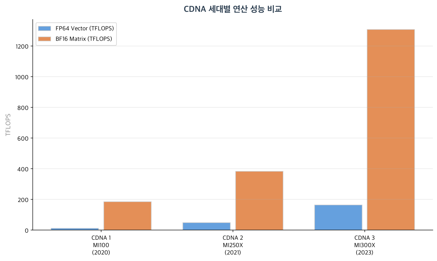
| CDNA 1 (MI100) | CDNA 2 (MI250X) | CDNA 3 (MI300X) | CDNA 4 (MI355X) | |
|---|---|---|---|---|
| Process | 7nm | N6 (6nm) | XCD 5nm / IOD 6nm | XCD N3P / IOD N6 |
| Die config | Monolithic | 2-die MCM | 8 XCD + 4 IOD | 8 XCD + 2 IOD |
| HBM | HBM2 32 GB | HBM2e 128 GB | HBM3 192 GB | HBM3E 288 GB |
| Memory BW | 1.23 TB/s | 3.2 TB/s | 5.3 TB/s | 8 TB/s |
| FP64 | 11.5 TFLOPS | 47.9 TFLOPS | ~163 TFLOPS | ~79 TFLOPS |
| BF16/FP16 | 184.6 TFLOPS | 383 TFLOPS | 1,307 TFLOPS | ~5,000 TFLOPS |
| FP8 | - | - | ~2,610 TFLOPS | ~10,000 TFLOPS |
| FP4 / MXFP4 | - | - | - | ~20,000 TFLOPS |
| Key innovation | Matrix Core | MCM, FP64 Matrix | XCD chiplets, CPU+GPU APU | MXFP formats, N3P |
| Supercomputer | - | Frontier (1st exascale) | El Capitan (Top500 #1, 2024) | - |
RDNA Summary
| RDNA 1 | RDNA 2 | RDNA 3 | RDNA 4 | |
|---|---|---|---|---|
| Launch | 2019 | 2020 | 2022 | 2025 |
| Process | 7nm | 7nm | GCD 5nm + MCD 6nm | 4nm |
| Die config | Monolithic | Monolithic | Chiplet (GCD+MCD) | Monolithic |
| Ray tracing | None | 1st-gen RA | 2nd-gen RA | 3rd-gen RA |
| Infinity Cache | None | 128 MB (Navi 21) | 96 MB (Navi 31) | 64 MB (Navi 48) |
| Flagship | RX 5700 XT | RX 6900 XT | RX 7900 XTX | RX 9070 XT |
| Key feature | WGP, PCIe 4.0 | Infinity Cache, DX12U | Chiplet, Dual-Issue | Monolithic return, FSR 4 |
Both lines are converging on chiplet designs: RDNA 3 split compute and memory into GCD+MCD; CDNA 2 used a 2-die MCM; CDNA 3 assembled 8 XCDs, 4 IODs, and 8 HBM3 stacks into a single OAM package. Die-level specialization and heterogeneous integration are AMD’s answer to the physical limits of monolithic scaling.
Deep-Dive Series
| # | Topic | Link |
|---|---|---|
| 1 | RDNA 1 — Wave32, WGP, Turing comparison | Read |
| 2 | RDNA 2 — Ray Accelerator, Infinity Cache, Ampere comparison | Read |
| 3 | RDNA 3 — Chiplet (GCD+MCD), Dual-Issue, Ada comparison | Read |
| 4 | RDNA 4 — Monolithic return, 3rd-gen RA, FSR 4, Blackwell comparison | Read |
| 5 | CDNA 1 — GCN inheritance, Matrix Core, A100 comparison | Read |
| 6 | CDNA 2 — MCM 2-die, FP64 Matrix, Frontier | Read |
| 7 | CDNA 3 — 3D stacking, unified GPU, MI300A APU, El Capitan | Read |