Series Roadmap
| # | Topic | Status |
|---|---|---|
| Overview | RDNA / CDNA Full Timeline | ✅ |
| 5 | CDNA 1 — GCN inheritance, Matrix Core, A100 comparison | ✅ |
| 6 | CDNA 2 — MCM 2-die, FP64 Matrix, Frontier | ✅ |
| 7 | CDNA 3 — MI300X, 3D stacking, unified GPU, ROCm 6 | ✅ |
What CDNA 2 Left, What CDNA 3 Changed
CDNA 2 (MI250X) surpassed the die limit with MCM and completed HPC with FP64 Matrix. But two fundamental problems remained.
- Split GPU: two GCDs appeared as separate GPUs to the OS. Programmers had to manage die-to-die data movement directly.
- Immature software: ROCm couldn’t keep up with CUDA, so competitive hardware was still constrained in real-world use.
CDNA 3 redesigned the entire hardware and software stack, including both of these. Its generational change is the largest in the CDNA series — and at its center is the MI300X, the device with which AMD first established itself as a real alternative to NVIDIA in the AI inference market.
This article centers on the MI300X. The HPC-oriented variant MI300A (a CPU+GPU APU) is covered separately later.
| Axis | CDNA 2 (MI250X) | CDNA 3 (MI300X) |
|---|---|---|
| Packaging | 2.5D MCM (side by side) | 3.5D (XCD 3D-stacked on IOD) |
| Logical GPU | 2 (split) | 1 (unified logical GPU) |
| Die role | GCD (compute+IO mixed) | XCD (compute) + IOD (IO/cache) split |
| Shared cache | None | 256 MB Infinity Cache (unified LLC) |
| Data formats | FP16/BF16/INT8 | + FP8, TF32 added |
| Memory | HBM2e 128 GB | HBM3 192 GB |
| Software | ROCm 4/5 (immature) | ROCm 6 (PyTorch/vLLM official) |
3.5D Packaging: Stacking XCDs on IODs
CDNA 3’s biggest hardware change is packaging. From CDNA 2’s 2.5D MCM (dies placed side by side on an interposer), it shifted to 3D hybrid bonding.
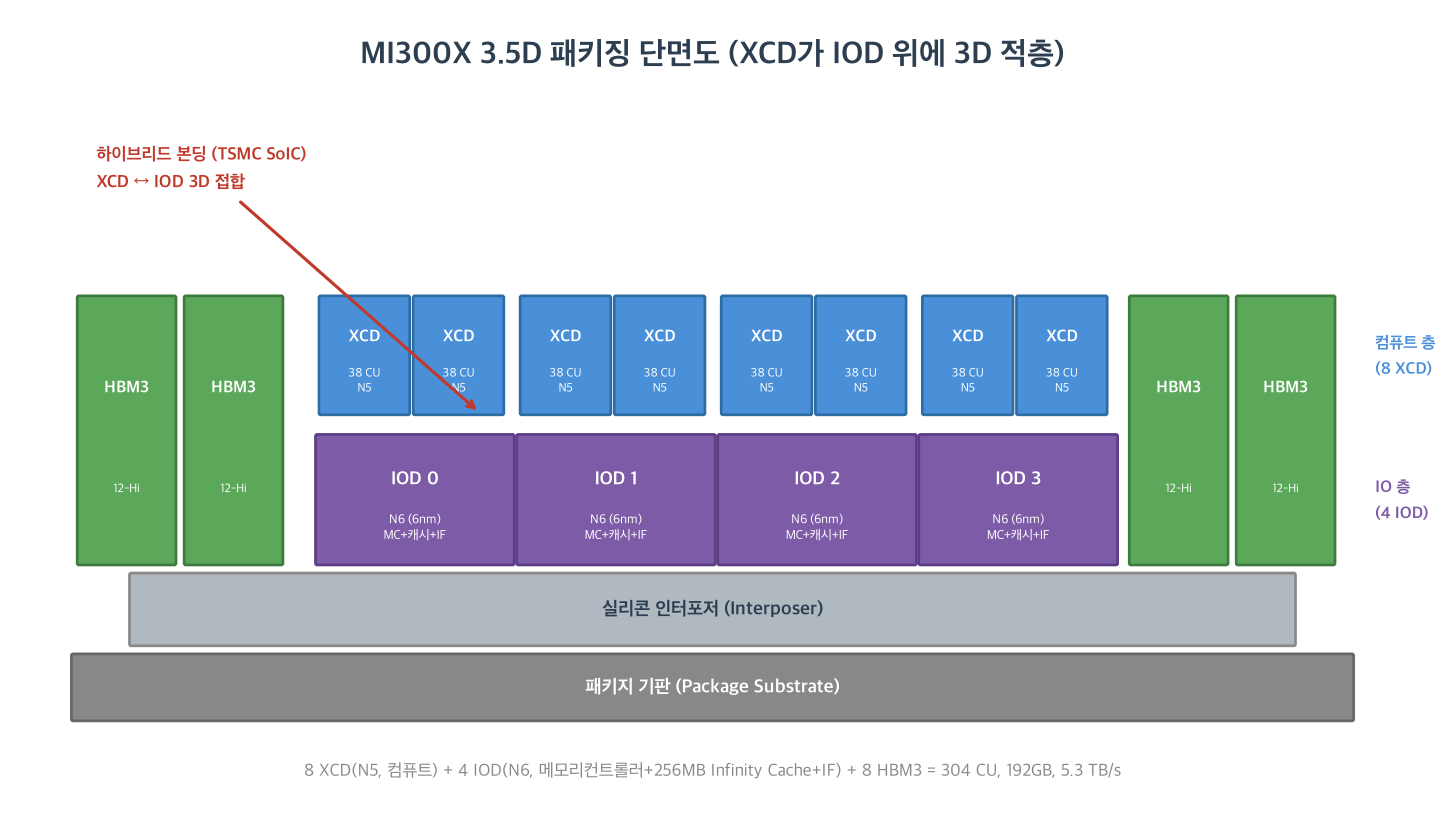
The MI300X stacks 12 dies into three layers.
- Compute layer: eight XCDs (Accelerator Complex Dies), TSMC N5 (5nm). Pure compute units only.
- IO layer: four IODs (I/O Dies), TSMC N6 (6nm). Memory controllers, Infinity Cache, and Infinity Fabric.
- Bonding: XCDs are 3D-bonded onto IODs via TSMC SoIC (hybrid bonding) — two XCDs per IOD.
It is called “3.5D” because it combines 2.5D (interposer) with 3D (die stacking). IODs and HBM3 sit on the interposer in 2.5D, while XCDs stack on IODs in 3D.
Separating Compute from IO
CDNA 2’s GCD mixed compute units and memory controllers on one die. CDNA 3 split them by role.
CDNA 2 GCD (mixed):            CDNA 3 (split):
┌─────────────────────┐        XCD (N5): compute only
│  CU + mem controller │              ↑ 3D bonding
│  + HBM PHY mixed     │        IOD (N6): memory controllers
└─────────────────────┘              + Infinity Cache + IF
The split brings two benefits. Compute logic (XCD) gains performance on the latest 5nm, while low-shrink IO/cache (IOD) stays on cheaper 6nm. And stacking XCDs directly on IODs minimizes the physical distance between compute and memory — shorter die-to-die wiring improves bandwidth and power efficiency.
Unified Logical GPU: Solving CDNA 2’s Homework
CDNA 2’s biggest usability problem was the MI250X appearing as two GPUs. CDNA 3 solved it fundamentally.
The MI300X’s eight XCDs share 256 MB of Infinity Cache through the four IODs. This shared cache provides a coherent last-level cache (LLC) across all XCDs, so the eight XCDs operate as one logical GPU.
CDNA 2 (MI250X):                 CDNA 3 (MI300X):
GPU0 ←IF→ GPU1                   ┌──────────────────────────┐
(separate addr spaces)           │ 256 MB Infinity Cache     │
programmer manages the split     │ shared by all 8 XCDs      │
                                │ → operates as 1 logical GPU│
                                │ → programmer treats as one │
                                └──────────────────────────┘
The programmer handles the MI300X as a single GPU, with no need to explicitly manage die-to-die partitioning. When desired, compute partitioning modes can split XCD groups into multiple logical GPUs. Unified is the default; splitting is optional — the exact opposite of CDNA 2.
Enhanced Matrix Core and FP8
CDNA 3 substantially strengthened Matrix Core and added low-precision formats for AI inference.
- FP8 added: 2,614 TFLOPS on the MI300X. The key format for LLM inference.
- TF32 added: the training-friendly format NVIDIA introduced on the A100 is now supported on CDNA 3.
- Throughput gains: 3× FP16/BF16 and 6.8× INT8 vs. CDNA 2 (AMD stated).
MI300X compute performance:
  FP64 vector  :   81.7 TFLOPS
  FP64 Matrix  :  163.4 TFLOPS
  FP32 vector  :  163.4 TFLOPS
  FP16/BF16    : 1307.4 TFLOPS
  FP8          : 2614.9 TFLOPS   ← new
Delivering both top-tier FP64 and FP8 is CDNA 3’s signature. FP64 targets HPC (scientific computing); FP8 targets AI (LLM inference). One architecture aims at both markets at once.
MI300X Specs:
| Item | Value |
|---|---|
| Process | XCD N5 (5nm) / IOD N6 (6nm) |
| Die config | 8 XCD + 4 IOD + 8 HBM3 (12 dies) |
| Transistors | ~153B |
| CUs | 304 (38 per XCD × 8) |
| Stream processors | 19,456 |
| Infinity Cache | 256 MB (shared LLC) |
| Memory | HBM3 192 GB (12-Hi) |
| Memory bandwidth | 5.3 TB/s |
| FP64 Matrix | 163.4 TFLOPS |
| FP8 | 2,614 TFLOPS |
| TDP | 750 W |
Why the MI300X Matters: 192GB on a Single Card
The reason the MI300X is CDNA 3’s key device lies not in benchmark numbers but in memory capacity — which is exactly what the AI inference market demanded.
In LLM inference, the biggest constraint is memory, not compute. Model weights and the KV cache must fit in GPU memory. The MI300X holds 192 GB of HBM3 on a single card. At the same time, NVIDIA’s H100 held 80 GB and the H200 held 141 GB.
GPUs needed to serve a 70B model (FP16 weights ~140 GB):
  H100 (80 GB)   : at least 2 cards (split via tensor parallelism)
  H200 (141 GB)  : 1 card (little headroom)
  MI300X (192 GB): 1 card (with KV cache headroom too)
When a large model fits on a single card, inter-GPU communication disappears. The overhead and complexity of tensor-parallel splitting shrink. Larger KV cache capacity means longer context and larger batches. Where inference throughput is directly service cost, this advantage is immediate.
Thanks to this, the MI300X became AMD’s first datacenter GPU to reach large-scale commercial adoption. Major clouds including Microsoft Azure offer MI300X instances. For the first time, a real alternative to NVIDIA’s monopoly appeared in the AI accelerator market.
The Software Upheaval: ROCm 6
The MI300X’s hardware advantage (192 GB, 5.3 TB/s) translated into real adoption because software backed it. ROCm 6, launched alongside CDNA 3, was as big a change as the hardware.
In the CDNA 1/2 era, ROCm’s biggest weakness was ecosystem maturity. Even with good hardware, framework support couldn’t keep up with CUDA. ROCm 6 narrowed that gap sharply.
Key changes:
- Official PyTorch support: PyTorch is officially supported on the MI300X. Standard workflows run without custom patches.
- vLLM integration: the LLM inference framework vLLM supports the MI300X. ROCm 6.2 added FP8 inference and FP8 KV cache.
- FP8 GEMM: FP8 matrix operations are accelerated in PyTorch and JAX through hipBLASLt.
- Container deployment: prebuilt Docker images bundling ROCm + vLLM + PyTorch simplified deployment.
ROCm 6 stack (MI300X inference):
  vLLM 0.6.x  (LLM serving, FP8 KV cache)
     │
  PyTorch 2.5 (framework)
     │
  hipBLASLt / Composable Kernel (FP8 GEMM)
     │
  ROCm 6.2 runtime + HIP
     │
  MI300X (CDNA 3)
In the CDNA 3 generation, AMD’s datacenter GPU had both hardware and software for the first time. The hardware strength of 192 GB was realized as real services on top of vLLM’s FP8 inference.
The Variant: MI300A APU
Built on the same CDNA 3 base but aimed at HPC, the MI300A is AMD’s first datacenter APU integrating CPU and GPU in a single package.
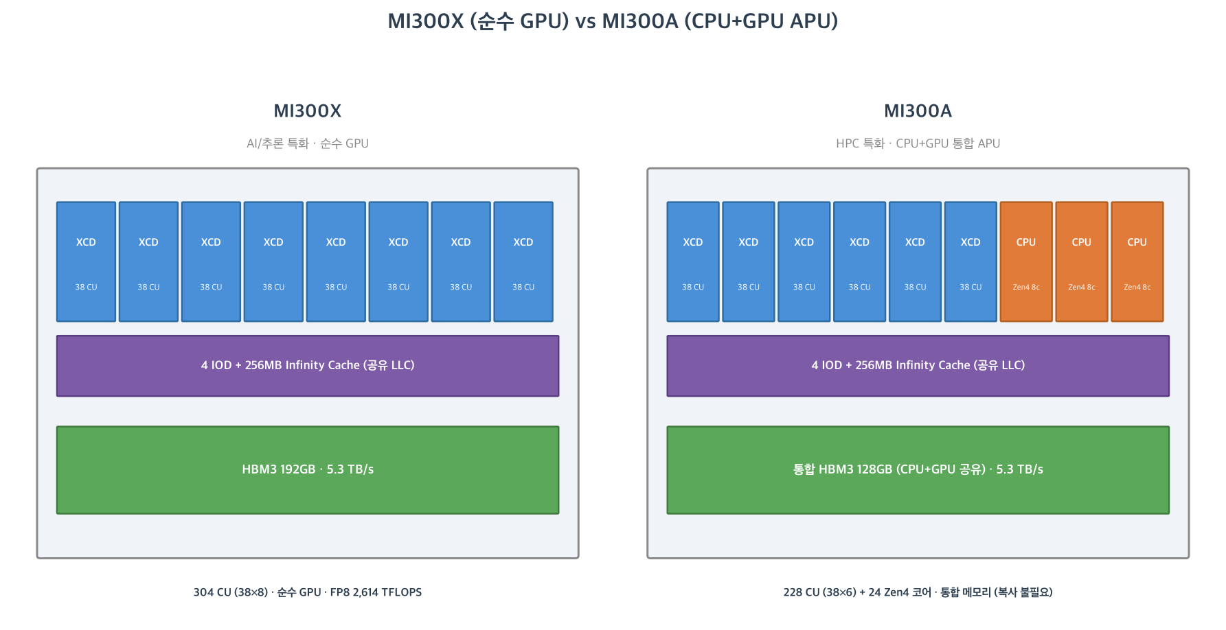
The MI300A replaces two of the MI300X’s XCDs with three Zen 4 CPU chiplets (CCDs).
- MI300X: 8 XCDs (pure GPU), HBM3 192 GB
- MI300A: 6 XCDs + 3 Zen 4 CCDs (24 CPU cores) + 228 CUs, unified HBM3 128 GB
The core idea is that CPU and GPU share the same HBM3 pool. Traditionally, passing a CPU-computed result to the GPU required an explicit copy. On the MI300A, CPU and GPU see the same address in the same physical memory. Data copies disappear, simplifying programming and improving performance in HPC workloads with frequent CPU-GPU interaction. The direction matches NVIDIA’s Grace-Hopper (GH200), but where GH200 is a two-chip link, the MI300A is single-package integration.
The MI300A is the compute engine of El Capitan, the Lawrence Livermore National Laboratory (LLNL) supercomputer that took Top500 #1 in November 2024 (1.742 EFlop/s HPL, 43,808 MI300A units). It is AMD’s second exascale #1 system, after CDNA 2’s Frontier.
The MI300 series later strengthened memory with MI325X (2024). Same CDNA 3 architecture, with HBM3 swapped for HBM3e — 256 GB capacity, 6.0 TB/s bandwidth, directly increasing KV cache capacity for LLM inference.
Comparison with NVIDIA H100/H200
The MI300X’s competitor is NVIDIA’s H100 (Hopper, 2022) and its memory-enhanced variant, the H200.
Specification Comparison
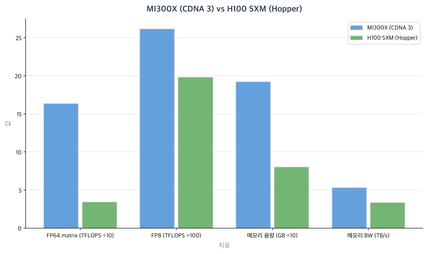
| MI300X (CDNA 3) | H100 SXM (Hopper) | H200 (Hopper) | |
|---|---|---|---|
| Process | N5 + N6 | TSMC 4N | TSMC 4N |
| Die config | 3.5D 12-die | Monolithic | Monolithic |
| FP64 Matrix | 163.4 TFLOPS | 34 TFLOPS | 34 TFLOPS |
| FP8 | 2,614 TFLOPS | 1,979 TFLOPS | 1,979 TFLOPS |
| Memory | HBM3 192 GB | HBM3 80 GB | HBM3e 141 GB |
| Memory bandwidth | 5.3 TB/s | 3.35 TB/s | 4.8 TB/s |
| Multi-GPU | Infinity Fabric | NVLink + NVSwitch | NVLink + NVSwitch |
| Software | ROCm 6 | CUDA | CUDA |
Domain Breakdown
Single-GPU Hardware
The MI300X leads. FP64 Matrix is about 4.8× the H100’s, memory capacity 2.4× (192 vs. 80 GB), and bandwidth higher too. Even against the H200, it leads on capacity (192 vs. 141 GB) and bandwidth (5.3 vs. 4.8 TB/s). Fitting a larger model on a single card is an advantage for LLM inference.
Multi-GPU Scaling
NVIDIA leads. NVLink and NVSwitch surpass AMD’s Infinity Fabric-based links in all-to-all GPU bandwidth. In large-scale distributed training, this difference affects scaling efficiency.
Software
CUDA still leads (the so-called CUDA moat). ROCm 6 greatly narrowed the gap for inference workloads, but CUDA retains an edge in training maturity and kernel-optimization breadth. The MI300X secured strong competitiveness in inference and is closing the gap in training.
Summary
| Axis | Change vs. CDNA 2 |
|---|---|
| Packaging | 2.5D MCM → 3.5D (XCD 3D-stacked on IOD) |
| Logical GPU | 2 split → 1 unified (256 MB Infinity Cache) |
| Die role | GCD mixed → XCD (compute) + IOD (IO) split |
| Data formats | FP16/BF16/INT8 → + FP8, TF32 |
| Memory | HBM2e 128 GB → HBM3 192 GB |
| Software | ROCm 4/5 → ROCm 6 (PyTorch/vLLM official) |
| Variant | - → MI300A APU (CPU+GPU unified memory), El Capitan |
| MI300X (CDNA 3) | H100/H200 (Hopper) | |
|---|---|---|
| FP64 Matrix | 163.4 TFLOPS (dominant) | 34 TFLOPS |
| Memory capacity | 192 GB (ahead) | 80 / 141 GB |
| Memory bandwidth | 5.3 TB/s (ahead) | 3.35 / 4.8 TB/s |
| Multi-GPU scaling | Behind | NVLink/NVSwitch (ahead) |
| Software | ROCm 6 (inference-competitive) | CUDA (ahead) |
CDNA 3 is the largest generational change in the CDNA series. Its key device, the MI300X, separated compute from IO with 3D stacking, resolved CDNA 2’s programming complexity with a unified logical GPU, and held a large model on a single card with 192 GB of HBM3. ROCm 6’s software maturity backed this hardware in production. The MI300X became AMD’s first datacenter GPU to be a real alternative to NVIDIA in the AI inference market. The HPC variant MI300A renewed the world #1 with El Capitan.
This concludes the AMD GPU architecture series (RDNA 1–4, CDNA 1–3). The successor CDNA 4 (MI350) is covered in the overview post.