The Problem: The Memory Wall
A server CPU socket has a fixed number of DIMM slots — typically 16 to 24, yielding at most a few terabytes of DRAM. AI inference workloads tell a different story: KV caches for 100B+ parameter models can demand hundreds of gigabytes. The number of concurrent requests a single inference server can handle ultimately hits the DRAM capacity ceiling.
At the same time, data movement between CPU and GPU remains non-coherent over PCIe. A GPU reading CPU memory requires explicit DMA, cache flush management, and driver-mediated synchronization. The CPU and GPU operate in separate coherency domains.
CXL (Compute Express Link) is an open interconnect standard that addresses both constraints simultaneously.
What Is CXL?
CXL is a high-speed interconnect protocol built on top of the PCIe physical layer. Intel introduced the initial specification in 2019; AMD, ARM, NVIDIA, Samsung, Micron, Alibaba, and others participate in the CXL Consortium.
Three goals:
- Memory capacity expansion: CPUs access memory attached to CXL devices beyond physical DIMM slot limits
- Cache coherency: accelerators participate in the CPU’s memory coherency domain without explicit copies
- Memory pooling: multiple servers share a common CXL memory pool dynamically
The physical layer is PCIe — PCIe 5.0 pins for CXL 1.x/2.0, PCIe 6.0 for CXL 3.0. CXL layers new transaction protocols on top of the shared PCIe link/physical layer.
Three Sub-Protocols
CXL defines three independent sub-protocols. A device’s type is determined by which subset it supports.
CXL Protocol Stack

┌──────────────────────────────────────────────┐
│  CXL.io      │  CXL.cache   │  CXL.mem       │  ← CXL transaction layer
├──────────────────────────────────────────────┤
│           CXL Flex Bus (ARB/MUX)             │  ← protocol multiplexer
├──────────────────────────────────────────────┤
│           PCIe 5.0 / 6.0 physical layer      │  ← shared physical link
└──────────────────────────────────────────────┘
CXL.io
A PCIe-compatible I/O protocol. Handles device discovery, enumeration, BAR mapping, and configuration space access. Existing PCIe drivers can detect CXL devices through this protocol without modification.
CXL.cache
Allows a device (accelerator) to coherently cache regions of host CPU memory.
Traditional PCIe DMA is non-coherent. A GPU reading CPU memory requires the driver to set up DMA transfers and explicitly manage CPU cache flushes. CXL.cache moves that responsibility to hardware.
PCIe (non-coherent):
CPU DRAM → explicit DMA copy → GPU buffer → GPU compute
  ↑ software manages cache coherency

CXL.cache (coherent):
CPU DRAM ← CXL.cache → accelerator
  ↑ hardware manages coherency automatically
  accelerator reads/writes CPU cache lines directly
The accelerator can hold CPU memory regions in its own cache. If the CPU modifies that data, the CXL.cache protocol sends MESI-style invalidation messages to the accelerator’s cache — the same mechanism that keeps multi-socket CPU caches coherent.
CXL.mem
Allows the host CPU to directly address memory attached to a CXL device.
The CPU maps CXL device memory into its physical address space. Standard malloc() and mmap() work on this memory. The OS exposes it as a separate NUMA node.
CPU physical address space with CXL.mem

[Local DRAM range]  0x0000_0000–0x3FFF_FFFF  → DDR5 DIMMs
[CXL.mem range]     0x4000_0000–0x7FFF_FFFF  → CXL Type 3 device DRAM
                    (exposed as NUMA node 1)
Device Types
| Type | Protocols | Purpose | Examples |
|---|---|---|---|
| Type 1 | CXL.io + CXL.cache | No attached memory; device caches host memory | SmartNIC, FPGA |
| Type 2 | CXL.io + CXL.cache + CXL.mem | Has memory; bidirectional coherency | GPU, AI accelerator |
| Type 3 | CXL.io + CXL.mem | Host memory expansion only | CXL DRAM module |
Type 3 is the form factor most actively shipping today. Samsung, Micron, and SK Hynix produce CXL DRAM modules that plug into a CXL slot and extend server memory capacity beyond DIMM limits, reaching multi-terabyte configurations per server.
Type 2 is the form factor where a GPU or AI accelerator participates in CPU cache coherency. Current-generation GPU products use PCIe without full CXL Type 2 coherency; this is an area of active development.
Version Evolution
CXL 1.0 / 1.1 (2019/2020)
PCIe 5.0 physical layer. Single host CPU connected to a single CXL device. All three protocols defined. Per-link bandwidth: ~64 GB/s (PCIe 5.0 x16).
Production CPU support:
- Intel Xeon Sapphire Rapids (4th gen, 2023): CXL 1.1
- AMD EPYC Genoa (9004 series, 2022): CXL 1.1
CXL 2.0 (2020)
Added CXL switches and memory pooling. A single switch connects multiple host servers to multiple CXL devices. Resources are partitioned and assigned dynamically.
CXL 2.0 pooling topology

  Host A ─┐                    ┌─ CXL DRAM 0 (256GB)
  Host B ─┤── CXL Switch ──────┤─ CXL DRAM 1 (256GB)
  Host C ─┘                    └─ CXL DRAM 2 (256GB)

Host A allocated 256GB, Host B 512GB, Host C 256GB — dynamically reassigned
Memory-intensive workloads (inference servers) and compute-intensive workloads (training servers) can draw from the same CXL pool, raising average utilization.
CXL 3.0 (2022)
Multi-level fabric and peer-to-peer (P2P) device communication. CXL switches can be connected hierarchically, supporting memory fabrics at thousands-of-nodes scale. PCIe 6.0 physical layer doubles per-link bandwidth to ~128 GB/s.
Latency Characteristics
CXL memory carries higher access latency than local DRAM. Protocol processing and link traversal add overhead.
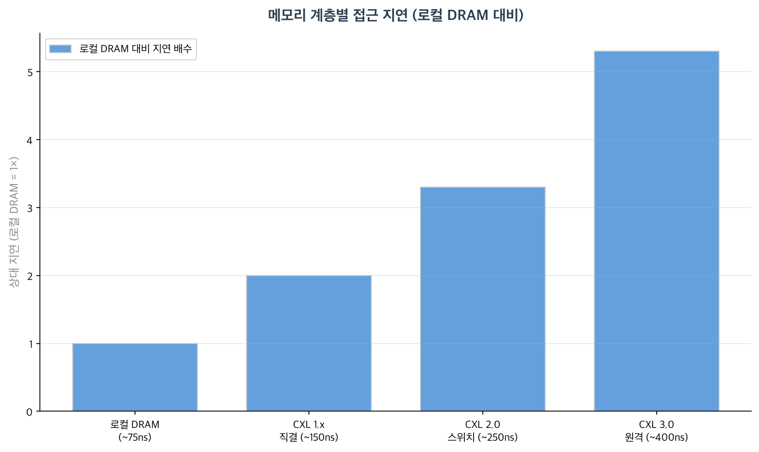
| Memory tier | Approximate latency | vs local DRAM |
|---|---|---|
| Local DRAM (DDR5) | ~75ns | 1× |
| CXL 1.x direct attach | ~150ns | ~2× |
| CXL 2.0 via switch | ~250ns | ~3× |
| CXL 3.0 remote node | ~400ns | ~5× |
The ~2× latency increase at direct attach is an acceptable tradeoff for many workloads. Bandwidth-bound workloads — notably LLM KV cache reads, which scan large memory ranges sequentially — are far less sensitive to latency than to total capacity and bandwidth.
The OS registers CXL memory as a separate NUMA node. Explicit placement via numactl --membind=1 or MAP_POPULATE directs allocations to CXL nodes. Linux 6.x includes a CXL subsystem that automates device discovery and NUMA node registration.
AI and LLM Use Cases
KV Cache Offloading
In LLM serving, KV cache size grows with batch size and sequence length. Model weights are fixed; KV cache is dynamic.
Example LLM serving memory layout (70B model, FP16)

GPU HBM (80GB):
  Model weights:  ~35GB
  KV cache:       ~20GB  ← limits concurrent requests
  Other:           ~5GB

With CXL memory expansion (256GB):
  Overflow KV cache: ~200GB  ← significantly more concurrent sequences
  (applied to historical tokens where latency is less critical)
Keeping only the most recent context tokens in GPU HBM while offloading historical KV cache to CXL memory allows a single GPU to serve more concurrent requests. Latency per token increases slightly for long-context queries but throughput improves.
Memory Pooling for Inference Clusters
Under CXL 2.0 pooling, multiple inference servers share a physical CXL memory pool. When one server’s load is low and its CXL allocation is underutilized, the capacity can be reassigned to a busier server dynamically — improving overall memory utilization across the fleet.
CXL vs NVLink vs PCIe
| PCIe | CXL | NVLink | |
|---|---|---|---|
| Physical layer | PCIe | PCIe (shared) | Proprietary |
| Standard | Open | Open | Proprietary (NVIDIA) |
| Cache coherency | None | Yes | Yes (NVLink-C2C) |
| Peak bandwidth | PCIe 5.0: ~64 GB/s | PCIe 6.0: ~128 GB/s | NVLink 5.0: 1,800 GB/s |
| Connection scope | General I/O | CPU to device/memory | GPU-to-GPU, GPU-to-CPU |
| Primary use | Universal I/O | Memory expansion + coherency | GPU cluster communication |
NVLink dominates on bandwidth but is NVIDIA-proprietary and GPU-centric. CXL is vendor-neutral and CPU-centric, suited for memory hierarchy extension. They are complementary rather than competing in practice — a server can use both: NVLink between GPUs and CXL for CPU memory expansion.
Ecosystem Status
| Component | Status |
|---|---|
| CPU support | Intel Xeon Sapphire Rapids/Granite Rapids (CXL 1.1/2.0), AMD EPYC Genoa/Turin (CXL 1.1/2.0) |
| CXL DRAM modules | Samsung CMM-D, Micron CZ120, SK Hynix AiMX (Type 3) |
| CXL switches | Microchip PFX, Astera Labs Leo (CXL 2.0 switching) |
| OS support | Linux 6.0+ (CXL subsystem), automatic NUMA node registration |
| AI frameworks | PyTorch / vLLM support NUMA-aware allocation; CXL nodes accessible via numactl |
Summary
| Item | Detail |
|---|---|
| Physical layer | PCIe 5.0 (CXL 1.x/2.0), PCIe 6.0 (CXL 3.0) |
| Core protocols | CXL.io (I/O), CXL.cache (coherent cache), CXL.mem (memory expansion) |
| Device types | Type 1 (cache only), Type 2 (cache + memory), Type 3 (memory expansion) |
| CXL 1.x | Point-to-point, single host |
| CXL 2.0 | Switching, memory pooling |
| CXL 3.0 | Multi-level fabric, P2P between devices |
| Latency overhead | ~2× (direct attach) to ~5× (remote) vs local DRAM |
| AI use cases | KV cache offloading, shared memory pools |
CXL extends the CPU-centric memory hierarchy to multi-terabyte scale over PCIe infrastructure, and resolves CPU-accelerator cache coherency at the hardware level. As LLM inference memory demands continue to grow, CXL adoption in AI infrastructure is accelerating.
References
- CXL Consortium. CXL Specification 3.0. computeexpresslink.org, 2022.
- Intel. Compute Express Link (CXL) Technology Overview. Intel Developer Zone, 2023.
- Linux Kernel. CXL Subsystem Documentation. kernel.org/doc/html/latest/driver-api/cxl.
- MemVerge. CXL Memory Tiering in AI Workloads. 2023.