Series Roadmap
| # | Topic |
|---|---|
| 1 | The Origins of GPU and the Birth of SIMT — Tesla, Fermi |
| 2 | Kepler and Maxwell — The Pursuit of Efficiency |
| 3 | Pascal — 16nm FinFET and the Arrival of NVLink |
| 4 | Volta — Tensor Cores and Independent Thread Scheduling |
| 5 | GPU Memory Systems and Optimization |
| 6 | GPU Internals — Pipelines and Execution Units |
What Maxwell Left Unfinished
On 28nm, Maxwell lifted per-core performance by 40% over Kepler through the SMM Quadrant redesign. But the physical ceiling of the 28nm process remained. GM200 filled 601mm² at 250W TDP — beyond that, adding more cores yielded diminishing returns.
The second constraint was memory bandwidth. Maxwell Titan X delivered 336 GB/s. PCIe 3.0 x16 provided roughly 31 GB/s bidirectional. Multi-GPU workloads had to move data through that bottleneck between GPUs.
Pascal (2016) addressed both simultaneously: a move to TSMC 16nm FinFET, HBM2 stacked memory, and the NVLink interconnect.
Process Transition and SM Redesign
Die Specifications
| GM200 (Maxwell) | GP100 | GP102 | GP104 | |
|---|---|---|---|---|
| Process | 28nm | 16nm FinFET | 16nm FinFET | 16nm FinFET |
| Transistors | 8.0B | 15.3B | ~12B | ~7.2B |
| Die Area | 601mm² | 610mm² | ~471mm² | ~314mm² |
| CUDA Cores / SM | 128 | 64 | 128 | 128 |
| SM Count | 24 | 60 | 28 | 20 |
| Compute Capability | 5.2 | 6.0 | 6.1 | 6.1 |
| Representative Products | Titan X ‘15 | Tesla P100 | GTX 1080 Ti | GTX 1080 |
The FinFET transition packed nearly twice the transistors into the same die area.
GP100: The 2 Processing Block Design
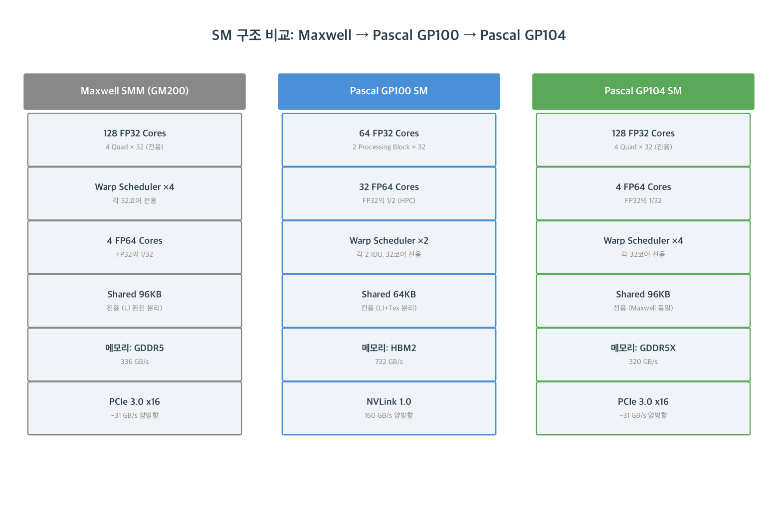
Unlike Maxwell SMM’s 4 Quadrants, each GP100 SM consists of 2 Processing Blocks. Each block contains one warp scheduler, 2 dispatch units, 32 FP32 cores, and 16 FP64 cores — all independent.
GP100 SM (64 FP32 + 32 FP64)
┌──────────────────────────────────────────┐
│  Processing Block 0                      │
│  Warp Scheduler  │  Dispatch Unit ×2    │
│  32 FP32 Cores   │  16 FP64 Cores      │
│  8 LD/ST Units   │  8 SFU              │
├──────────────────────────────────────────┤
│  Processing Block 1                      │
│  Warp Scheduler  │  Dispatch Unit ×2    │
│  32 FP32 Cores   │  16 FP64 Cores      │
│  8 LD/ST Units   │  8 SFU              │
├──────────────────────────────────────────┤
│  Shared Memory 64KB  │  L1+Tex (separate) │
│  Register File 256KB (65K×32b)           │
└──────────────────────────────────────────┘
The FP32-to-scheduler ratio stays at 32:1 — matching Maxwell’s Quadrant philosophy. The key change is the FP64 ratio: GM200 carried 4 FP64 cores per SM (1/32 of FP32), while GP100 carries 32 (1/2 of FP32). This directly targets HPC scientific workloads.
GP100 SM supports up to 64 warps/SM, 32 blocks/SM in-flight simultaneously.
GP102 and GP104 retain Maxwell SMM’s 4 Quadrant, 128-core layout. FP64 cores remain at 4 per SM (1/32 ratio), keeping FP64 performance minimal for consumer use.
HBM2 and NVLink — Redefining Bandwidth
HBM2 (GP100 Exclusive)
GP100 integrates HBM2 stacks directly within the package, replacing external GDDR memory.
GP100 Package Layout
┌────────────────────────────────────────────┐
│  GPU Die ──┬── HBM2 Stack 0 (4GB)          │
│            ├── HBM2 Stack 1 (4GB)          │
│            ├── HBM2 Stack 2 (4GB)          │
│            └── HBM2 Stack 3 (4GB)          │
│                                            │
│  Bus Width: 4,096-bit (1,024-bit per stack) │
│  Total VRAM: 16 GB                         │
│  Peak Bandwidth: 732 GB/s                  │
└────────────────────────────────────────────┘
This is 2.2× the Maxwell GM200 (336 GB/s) and 2.3× the GP104 GDDR5X (320 GB/s).
NVLink 1.0 (GP100 Exclusive)
| PCIe 3.0 x16 | NVLink 1.0 (GP100) | |
|---|---|---|
| Links | — | 4 |
| Bandwidth per Link | — | 20 GB/s bidirectional |
| Total Bandwidth | ~31 GB/s | 160 GB/s |
| Multiplier | 1× | ~5× |
NVLink replaces PCIe as the GPU-to-GPU interconnect. The 8 P100s in a DGX-1 server form a mesh topology over NVLink, removing the PCIe bottleneck from AllReduce communication.
FP16 — The Foundation for Deep Learning Acceleration
GP100 supports the half2 vector type, packing two FP16 values into a single 32-bit register and processing both in one clock cycle.
| FP64 | FP32 | FP16 | |
|---|---|---|---|
| P100 SXM2 (TFLOPS) | 5.3 | 10.6 | 21.2 |
| Ratio vs FP32 | 0.5× | 1× | 2× |
#include <cuda_fp16.h>
__global__ void fp16_fma(half2 *a, half2 *b, half2 *c, half2 *d) {
    int i = threadIdx.x;
    d[i] = __hfma2(a[i], b[i], c[i]);  // Two FP16 FMAs in one clock
}
On GP102/GP104 (CC 6.1), FP16 throughput is 1/64 of FP32 — effectively software emulation. INT8 dot product (__dp4a) on CC 6.1, however, delivers the same throughput as FP32.
GP100’s native FP16 was the only hardware basis for mixed-precision training before Volta’s Tensor Cores arrived in 2017.
Unified Memory’s Leap Forward
Maxwell’s Constraints
Memory allocated with cudaMallocManaged() under Maxwell was eagerly migrated — all pages were moved to the GPU before kernel launch. Datasets exceeding GPU memory capacity were impossible. CPU and GPU accessing the same managed memory simultaneously caused segfaults.
Pascal: The Page Migration Engine
When a GPU thread accesses a non-resident page, the Page Migration Engine raises a fault to the OS. The OS migrates only that page to the GPU; the thread resumes.
Maxwell: Eager Migration             Pascal: On-demand Migration
────────────────────────             ────────────────────────────────
Before kernel launch:                During kernel execution:
  All managed pages migrated           Thread → non-resident page access
  to GPU in bulk                           → Page Migration Engine
                                           → OS fault → that page only
                                           → Thread resumes

GPU oversubscription: impossible  →  possible
CPU concurrent access: impossible →  possible
Virtual address space: GPU mem    →  49-bit (512 TB, CPU+GPU)
CUDA 8.0 added two new APIs:
// Async prefetch — overlaps with compute
cudaMemPrefetchAsync(data, size, device_id, stream);

// Memory access pattern hints
cudaMemAdvise(data, size, cudaMemAdviseSetReadMostly, device_id);
// read-mostly regions are automatically replicated to both CPU and GPU
On P100 systems with NVLink, oversubscribed datasets incur only about 30% throughput loss compared to in-core execution. NVLink’s bandwidth absorbs most of the page migration cost. PCIe systems see higher overhead.
Compute Preemption
Maxwell only supported context switching at CUDA block boundaries. A compute kernel running for multiple seconds locked out graphics rendering entirely.
Pascal (CC 6.x — GP100, GP102, GP104) introduces instruction-level preemption: the kernel can be interrupted at any instruction boundary and its context saved. Compute and graphics time-slice on a single GPU. Interactive kernel debugging also becomes viable.
Interconnect and External Channels
PCIe Host Interface
GP102/GP104 consumer GPUs use PCIe 3.0 x16 (16 GB/s unidirectional) as the host interface. GP100 (P100) also carries PCIe 3.0 x16 for host connectivity; NVLink 1.0 handles GPU-to-GPU traffic separately.
L2 Cache
| Die | L2 Cache |
|---|---|
| GP100 (P100) | 4 MB |
| GP102 (GTX 1080 Ti) | ~3.5 MB |
| GP104 (GTX 1080) | 2 MB |
NVENC / NVDEC
| GP100 (P100) | GP102 / GP104 (Consumer) | |
|---|---|---|
| NVENC | None | 3rd gen (H.264, HEVC 10-bit) |
| NVDEC | None | 3rd gen (HEVC 10-bit decode) |
| Display outputs | None | Yes |
GP100 is a datacenter card — no NVENC, NVDEC, or display outputs. Consumer Pascal (GP102/GP104) includes 3rd-gen NVENC/NVDEC with HEVC 10-bit encode and decode.
Display Outputs (consumer reference cards)
| Product | DP | HDMI | DVI |
|---|---|---|---|
| GTX 1080 Ti (GP102) | 1.4 ×3 | 2.0b ×1 | DVI-D ×1 |
| GTX 1080 (GP104) | 1.4 ×3 | 2.0b ×1 | DVI-D ×1 |
Summary
| Maxwell GM200 | Pascal GP100 | Pascal GP104 | |
|---|---|---|---|
| Process | 28nm | 16nm FinFET | 16nm FinFET |
| CUDA Cores / SM | 128 (4 Quad) | 64 (2 PB) | 128 (4 Quad) |
| FP64 Ratio | 1/32 | 1/2 | 1/32 |
| Memory | GDDR5 336 GB/s | HBM2 732 GB/s | GDDR5X 320 GB/s |
| L2 cache | 3 MB | 4 MB | 2 MB |
| PCIe | 3.0 x16 | 3.0 x16 | 3.0 x16 |
| GPU Interconnect | PCIe ~31 GB/s | NVLink 160 GB/s | PCIe ~31 GB/s |
| Native FP16 | None | 2× FP32 | None |
| NVENC | None | None | 3rd gen |
| Unified Memory | Eager migration | Page fault engine | Page fault engine |
| Compute Preemption | Block-level | Instruction-level | Instruction-level |
Pascal bifurcated into two distinct products. GP100 is an HPC/AI accelerator with HBM2, NVLink, native FP16, and substantial FP64 throughput. GP102 and GP104 inherit Maxwell’s Quadrant design for the consumer market.
The next post covers Volta — the introduction of Tensor Cores, NVLink 2.0, and the architecture that became the template for modern AI accelerators.
References
- NVIDIA. Inside Pascal: NVIDIA’s Newest Computing Platform. NVIDIA Developer Blog, 2016. Link
- NVIDIA. NVIDIA Tesla P100 GPU Architecture Whitepaper, 2016. PDF
- NVIDIA. Beyond GPU Memory Limits with Unified Memory on Pascal. NVIDIA Developer Blog, 2016. Link
- NVIDIA. Pascal Tuning Guide. CUDA Toolkit Documentation. Link
- NVIDIA. CUDA 8 Features Revealed. NVIDIA Developer Blog, 2016. Link
- NVIDIA. Mixed-Precision Programming with CUDA 8. NVIDIA Developer Blog, 2016. Link