Series Roadmap
| # | Topic |
|---|---|
| 1 | The Origins of GPU and the Birth of SIMT — Tesla, Fermi |
| 2 | Kepler and Maxwell — The Pursuit of Efficiency |
| 3 | Pascal — 16nm, HBM2, NVLink |
| 4 | Volta — Tensor Cores and Independent Thread Scheduling |
| 5 | Turing — RT Cores and 2nd-Gen Tensor Cores |
| 6 | GPU Memory Systems and Optimization |
What Pascal Left Open
Pascal GP100 addressed bandwidth through HBM2 (732 GB/s) and multi-GPU connectivity through NVLink (160 GB/s), and added native FP16 throughput at 2× FP32. But by 2016, the dominant computation in deep learning was unambiguous: general matrix multiply (GEMM).
Every major layer in a Transformer — multi-head attention projections, feedforward layers, output embeddings — reduces to D = A × B + C. Pascal’s FP32 CUDA Cores execute one scalar FMA per clock. FP16 half2 doubles the throughput, but the fundamental unit of work remains a single scalar multiply-add. Computing one element of an M×K × K×N product requires K sequential FMAs on a CUDA Core.
Volta (GV100, 2017) moved that inner K-loop into dedicated silicon.
Tensor Core: Dedicated Matrix Multiply Hardware
The 4×4 MMA Operation
A Tensor Core performs a 4×4 matrix multiply-accumulate (MMA) in a single clock cycle:
D[4×4] = A[4×4] × B[4×4] + C[4×4]

A, B: FP16 inputs
C:    FP32 accumulator
D:    FP32 result
A 4×4 matrix multiply produces 16 output elements, each a length-4 dot product: 16 × 4 FMA = 64 FP16 FMAs = 128 FP16 FLOPS per clock per Tensor Core.
One CUDA Core performs 2 FLOPS per clock (one FP16 FMA). One Tensor Core delivers 64× more FP16 throughput.
GV100 has 8 Tensor Cores per SM. Per-SM FP16 throughput:
| Unit | Count/SM | FP16 FLOPS/clock |
|---|---|---|
| FP32 CUDA Cores (half2) | 64 | 128 |
| Tensor Cores | 8 | 1,024 |
GV100 chip-wide (80 SMs, 1.53 GHz boost):
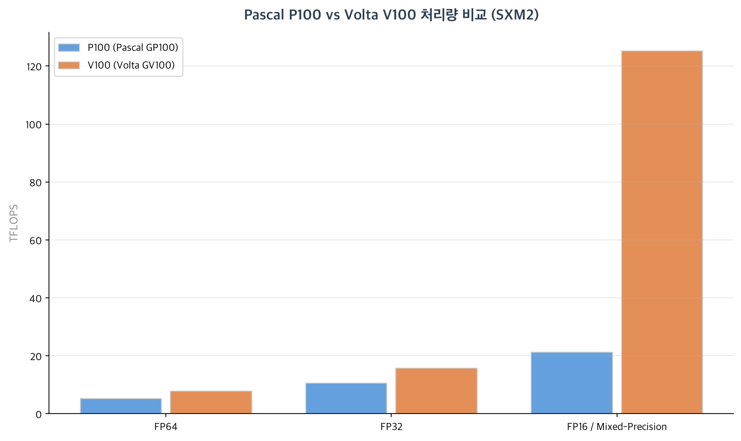
CUDA Core FP16:  128 × 80 × 1.53 GHz ≈  15.7 TFLOPS
Tensor Core FP16: 1,024 × 80 × 1.53 GHz ≈ 125.3 TFLOPS
Pascal P100 achieved 21.2 TFLOPS FP16 — roughly 6× less than V100 Tensor Core throughput.
Mixed-Precision Data Types
First-generation Tensor Cores (GV100, Compute Capability 7.0) support:
| Input (A, B) | Accumulator (C, D) |
|---|---|
| FP16 | FP32 |
| FP16 | FP16 |
FP32 accumulation preserves numerical range during intermediate sums — the hardware basis for mixed-precision training. Gradients stay in FP16, weight updates accumulate in FP32 master copies, and loss scaling keeps gradients in-range. cuBLAS and cuDNN automatically select Tensor Cores when operands are FP16 and sizes are multiples of 16.
GV100 SM: 4 Sub-core Design
Sub-core Partitioning
Pascal GP100 used 2 Processing Blocks per SM, each with a dual-issue Warp Scheduler and 32 FP32 + 16 FP64 cores. Volta GV100 restructures this into 4 sub-cores, each with a single-issue Warp Scheduler:
GV100 SM (4 Sub-cores)
┌──────────────────────────────────────────────────────┐
│  Sub-core 0                                          │
│  ┌──────────────────────────────────────────────┐    │
│  │ L0 Instruction Cache (new)                   │    │
│  │ Warp Scheduler  │  Dispatch Unit (×1)        │    │
│  ├─────────────────┼──────────────────────────  ┤    │
│  │  16 FP32 Cores  │  16 INT32 Cores (new)      │    │
│  │   8 FP64 Cores  │   2 Tensor Cores (new)     │    │
│  │   8 LD/ST Units │   4 SFU                    │    │
│  └─────────────────┴──────────────────────────  ┘    │
├──────────────────────────────────────────────────────┤
│  Sub-cores 1–3  (identical configuration)            │
├──────────────────────────────────────────────────────┤
│  Unified L1 / Shared Memory  128 KB                  │
│  Register File  256 KB (65,536 × 32-bit)             │
└──────────────────────────────────────────────────────┘

SM totals: 64 FP32, 64 INT32, 32 FP64, 8 TC, 32 LD/ST, 16 SFU

GV100 SM supports up to **64 warps/SM, 32 blocks/SM** in-flight. Register file: 256 KB/SM.
Pascal GP100 vs. Volta GV100
| Pascal GP100 | Volta GV100 | |
|---|---|---|
| SM sub-unit | Processing Block × 2 | Sub-core × 4 |
| FP32 / SM | 64 | 64 |
| FP64 / SM | 32 | 32 |
| INT32 / SM | shared with FP32 | 64 (dedicated) |
| Tensor Core / SM | none | 8 |
| Warp Scheduler / SM | 2 | 4 |
| Dispatch / Scheduler | 2 (dual-issue) | 1 (single-issue) |
| LD/ST / SM | 16 | 32 |
| SFU / SM | 8 | 16 |
| L0 Instruction Cache | none | per sub-core |
| L1 + Shared Memory | 64 KB + 64 KB (separate) | Unified 128 KB |
| Max Shared Memory | 64 KB | 96 KB |
Total dispatch slots per SM: Pascal GP100 had 2 × 2 = 4, Volta GV100 has 4 × 1 = 4 — identical throughput, redistributed across four independent sub-cores to support per-thread scheduling.
FP32/INT32 Dual Pipelines
Pascal’s FP32 units handled both floating-point and integer operations — integer work like loop counter increments and address arithmetic competed with FP32 for execution slots. Volta adds dedicated INT32 units that run concurrently with FP32:
Pascal: INT32 and FP32 share units
Cycle 1: FP32 FMA(A[i] × B[i])  →  INT32 IADD(i++) waits
Cycle 2: INT32 IADD completes    →  FP32 waits

Volta: Concurrent execution
Cycle 1: FP32 FMA(A[i] × B[i])  ║  INT32 IADD(i++)
Cycle 2: FP32 FMA(...)           ║  INT32 CMP / BRANCH
GEMM inner loops — where FP multiply-adds and integer loop control overlap naturally — benefit directly from this parallelism.
L0 Instruction Cache
Each sub-core receives its own L0 instruction cache, storing recently decoded instructions to reduce pressure on the shared L1 instruction cache. Tight loops no longer need an L1 fetch on every iteration.
Unified L1/Shared Memory
Pascal GP100 allocated 64 KB each to L1 and Shared Memory as separate banks. GV100 unifies them into a configurable 128 KB pool:
Shared Memory  |  L1 Cache
───────────────────────────
      0 KB     |  128 KB
     32 KB     |   96 KB
     64 KB     |   64 KB
     96 KB     |   32 KB   ← max shared memory
96 KB max (vs. Pascal’s 64 KB cap) enables larger GEMM tiles — fewer round-trips to HBM2 per output tile.
cudaFuncSetAttribute(my_kernel,
    cudaFuncAttributeMaxDynamicSharedMemorySize,
    96 * 1024);
Independent Thread Scheduling
This is the most significant microarchitectural change in Volta.
The Warp-Shared PC (Pascal and Earlier)
From Tesla through Pascal, 32 threads in a warp shared a single Program Counter. Branch divergence triggered the Active Mask mechanism: hardware serialized each taken path with non-participants masked, then reconverged at a compiler-inserted IPDOM (Immediate Post-Dominator) point.
The structural consequence: no fine-grained synchronization within a warp. Threads always advance together or stall together — intra-warp producer-consumer patterns are impossible.
Some Pascal-era code relied implicitly on this lock-step property: writing to shared memory then reading a neighboring thread’s value without __syncthreads(). This was undefined behavior that happened to work because threads were always in lock-step.
Per-Thread PC and Call Stack
Volta gives each thread its own Program Counter and call stack:
Pascal — one PC per warp:
  T0, T1, ..., T31 → shared PC → same instruction every cycle

Volta — one PC per thread:
  T0:  PC_0,  Stack_0
  T1:  PC_1,  Stack_1
  ...
  T31: PC_31, Stack_31

  Scheduler detects convergence at runtime:
  → convergent threads grouped into lock-step execution
  → divergent threads proceed independently
Convergent threads still execute in lock-step for efficiency. Volta’s scheduler performs runtime convergence detection — threads reaching the same PC are automatically bundled, unlike Pascal’s static IPDOM points inserted by the compiler. This also means stalled threads (e.g., waiting on memory) no longer hold back other threads in the same warp that are ready to execute.
__syncwarp() for Explicit Intra-Warp Fences
Code relying on implicit lock-step synchronization may produce incorrect results on Volta. CUDA 9.0 introduces __syncwarp(mask):
// ❌ Implicit lock-step assumption — unsafe on Volta
shmem[threadIdx.x] = val;
other = shmem[(threadIdx.x + 1) % 32];  // may read stale data

// ✅ Volta-safe
shmem[threadIdx.x] = val;
__syncwarp();          // all writes visible before any read proceeds
other = shmem[(threadIdx.x + 1) % 32];
The optional mask argument (uint32_t bitmask) specifies participating threads. __syncwarp() is equivalent to __syncwarp(0xffffffff).
Intra-Warp Producer-Consumer
Independent thread scheduling unlocks patterns that deadlocked on Pascal:
__shared__ float buf[16];

if (threadIdx.x < 16) {
    buf[threadIdx.x] = compute();
    __syncwarp(0x0000ffff);   // producers signal completion
} else {
    __syncwarp(0xffff0000);   // consumers participate in the fence
    float v = buf[threadIdx.x - 16];
    consume(v);
}
Threads 0–15 and 16–31 progress independently, synchronizing only at the __syncwarp boundary. On Pascal, this would deadlock.
NVLink 2.0 and Memory
NVLink 2.0
| NVLink 1.0 (GP100) | NVLink 2.0 (GV100) | |
|---|---|---|
| Links / GPU | 4 | 6 |
| Per-link bandwidth | 20 GB/s bidirectional | 25 GB/s bidirectional |
| Total bandwidth | 160 GB/s | 300 GB/s |
| NVSwitch | no | yes |
NVSwitch — introduced with DGX-2 (2018) — is a switching ASIC that fully connects 16 V100 GPUs through 12 NVSwitch chips. Every GPU pair communicates at full 300 GB/s, eliminating the ring-topology bottleneck of DGX-1.
HBM2 and L2
| Pascal P100 SXM2 | Volta V100 SXM2 | |
|---|---|---|
| VRAM | 16 GB | 16 / 32 GB |
| Bus width | 4096-bit | 4096-bit |
| HBM2 bandwidth | 732 GB/s | 900 GB/s |
| L2 Cache | 4 MB | 6 MB |
The 23% bandwidth increase and 50% larger L2 keep pace with the ~6× jump in Tensor Core compute throughput, preventing the memory subsystem from becoming the new bottleneck.
CUDA 9.0 Software Changes
Cooperative Groups
__syncthreads() synchronized an entire thread block with no way to express smaller or larger scopes. Cooperative Groups (CUDA 9.0) lets the programmer name the synchronization domain explicitly:
#include <cooperative_groups.h>
namespace cg = cooperative_groups;

__global__ void warp_reduce(float *in, float *out) {
    auto block = cg::this_thread_block();
    auto warp  = cg::tiled_partition<32>(block);

    float v = in[blockIdx.x * blockDim.x + threadIdx.x];

    for (int i = warp.size() / 2; i > 0; i /= 2)
        v += warp.shfl_down(v, i);

    if (warp.thread_rank() == 0)
        atomicAdd(out, v);
}
For grid-level barriers, cudaLaunchCooperativeKernel() guarantees all blocks are simultaneously resident, allowing cg::this_grid().sync() to act as a true grid-wide barrier — enabling multi-pass algorithms in a single kernel launch.
WMMA API
nvcuda::wmma exposes Tensor Cores at warp granularity — 32 threads collectively execute a 16×16×16 FP16 matrix multiply:
#include <mma.h>
using namespace nvcuda::wmma;

__global__ void wmma_mm(half *A, half *B, float *C, int M, int N, int K) {
    int warpRow = (blockIdx.y * blockDim.y + threadIdx.y);
    int warpCol = (blockIdx.x * blockDim.x + threadIdx.x) / warpSize;

    fragment<matrix_a, 16,16,16, half,  row_major> a_frag;
    fragment<matrix_b, 16,16,16, half,  col_major> b_frag;
    fragment<accumulator, 16,16,16, float>          acc;
    fill_fragment(acc, 0.0f);

    for (int k = 0; k < K; k += 16) {
        load_matrix_sync(a_frag, A + warpRow*16*K + k,   K);
        load_matrix_sync(b_frag, B + k*N + warpCol*16,   N);
        mma_sync(acc, a_frag, b_frag, acc);
    }
    store_matrix_sync(C + warpRow*16*N + warpCol*16, acc, N, mem_row_major);
}
mma_sync() distributes the 16×16×16 operation across the 32 warp threads’ registers; the Tensor Core hardware assembles the fragments into 4×4 MMA operations internally. In production, cuBLAS cublasGemmEx() and cuDNN handle Tensor Core scheduling automatically.
Interconnect and External Channels
PCIe Host Interface
The V100 PCIe card connects to the host via PCIe 3.0 x16 (16 GB/s unidirectional). The SXM2 form factor also uses PCIe 3.0 for host connectivity; NVLink 2.0 handles GPU-to-GPU traffic.
L2 Cache Topology
GV100’s 6 MB L2 is a single unified partition — all SMs access it symmetrically through a shared crossbar. This contrasts with Ampere A100’s 40 MB split into two physically separate 20 MB partitions.
External Channels
GV100 is a datacenter-only accelerator. The following are intentionally absent:
| Feature | Status |
|---|---|
| NVENC | None |
| NVDEC | None |
| Display outputs | None |
No consumer Volta product was released. The Titan V (2017) uses GV100 but also omits NVENC, NVDEC, and display outputs.
Summary
| Pascal GP100 | Volta GV100 | |
|---|---|---|
| Process | 16nm FinFET | 12nm FFN |
| Transistors | 15.3B | 21.1B |
| Die size | 610 mm² | 815 mm² |
| SMs | 60 | 80 |
| SM sub-unit | Processing Block × 2 | Sub-core × 4 |
| Tensor Core / SM | none | 8 |
| INT32 pipeline | shared with FP32 | dedicated, concurrent |
| FP16 throughput | 21.2 TFLOPS | 125.3 TFLOPS |
| FP32 throughput | 10.6 TFLOPS | 15.7 TFLOPS |
| FP64 throughput | 5.3 TFLOPS | 7.8 TFLOPS |
| LD/ST / SM | 16 | 32 |
| L0 Instruction Cache | none | per sub-core |
| Max Shared Memory | 64 KB | 96 KB |
| HBM2 bandwidth | 732 GB/s | 900 GB/s |
| L2 Cache | 4 MB | 6 MB |
| NVLink | 1.0, 160 GB/s | 2.0, 300 GB/s |
| PCIe | 3.0 x16 | 3.0 x16 |
| Max warps / SM | 64 | 64 |
| Max blocks / SM | 32 | 32 |
| NVENC | None | None |
| Thread scheduling | warp-shared PC | per-thread PC |
| TDP (SXM2) | 300 W | 300 W |
Volta’s changes fall into two categories. Tensor Cores and the dedicated INT32 pipeline extend throughput within the existing CUDA Core paradigm — additive hardware for specific workloads. Independent thread scheduling breaks a structural constraint that had been part of the SIMT model since Tesla — that threads within a warp either all execute or all stall together. These two directions set the foundation for Turing and Ampere: second- and third-generation Tensor Cores with INT8/INT4 support, RT Cores, and a progressively richer warp-level programming model.
The next post covers Turing: RT Cores, INT8/INT4 Tensor Cores, and the first consumer GPU with dedicated AI and ray-tracing acceleration.
References
- NVIDIA. NVIDIA Tesla V100 GPU Architecture Whitepaper. 2017. PDF
- NVIDIA. Inside Volta: The World’s Most Advanced Data Center GPU. NVIDIA Developer Blog, 2017.
- NVIDIA. Programming Tensor Cores in CUDA 9. NVIDIA Developer Blog, 2017.
- NVIDIA. CUDA 9 Features Revealed: Volta, Cooperative Groups and More. NVIDIA Developer Blog, 2017.
- Jia, Z. et al. Dissecting the NVIDIA Volta GPU Architecture via Microbenchmarking. arXiv:1804.06826, 2018.
- NVIDIA. CUDA C++ Best Practices Guide. Developer Documentation.