Series Roadmap
| # | Topic | Status |
|---|---|---|
| Overview | RDNA / CDNA Full Timeline | ✅ |
| 1 | RDNA 1 — Wave32, WGP, 7nm | ✅ |
| 2 | RDNA 2 — Ray Accelerator, Infinity Cache, Ampere comparison | ✅ |
| 3 | RDNA 3 — Chiplet (GCD+MCD), Dual-Issue, Ada comparison | ✅ |
| 4 | RDNA 4 — Monolithic return, 3rd-gen RA, FSR 4, Blackwell comparison | ✅ |
The Wall RDNA 2 Hit
RDNA 2 placed 128 MB of Infinity Cache on-die to work around GDDR6’s bandwidth ceiling. The problem: that approach becomes an obstacle in the next generation.
SRAM (cache) does not benefit from process shrinks the way logic does. Moving from 7nm to 5nm shrinks logic transistors dramatically, but SRAM cell area barely changes. Growing Infinity Cache further means letting SRAM consume expensive 5nm die area.
Memory controllers and PHYs face the same issue. These blocks are closer to analog circuits and gain little area from finer nodes. Putting non-scaling circuits on costly 5nm wafers is inefficient.
RDNA 3 (Navi 31, December 2022) solved this with chiplets.
Chiplets: The First Consumer GPU Die Split
RDNA 3 is AMD’s first chiplet-based consumer GPU. A single large die is split by function.
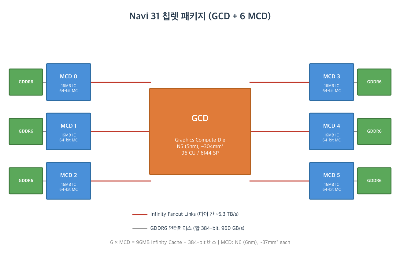
- GCD (Graphics Compute Die): shaders, Ray Accelerators, geometry engines, display engine, media engines. Logic-intensive, so it uses TSMC N5 (5nm). ~304 mm² on Navi 31.
- MCD (Memory Cache Die): 16 MB Infinity Cache + 64-bit GDDR6 memory controller each. Low shrink benefit, so it uses the cheaper TSMC N6 (6nm). ~37 mm² each.
Navi 31 pairs one GCD with six MCDs.
Split rationale:
┌─────────────────────────────┬────────────────────────────────┐
│  GCD (N5, 5nm)              │  MCD × 6 (N6, 6nm)             │
│  - Logic-intensive (shaders)│  - SRAM/analog (cache/PHY)     │
│  - High shrink benefit      │  - Low shrink benefit          │
│  → on expensive 5nm         │  → split out to cheaper 6nm    │
└─────────────────────────────┴────────────────────────────────┘

6 MCDs combined:
  Infinity Cache: 16 MB × 6 = 96 MB
  Memory bus: 64-bit × 6 = 384-bit → GDDR6 960 GB/s
The dies connect via Infinity Fanout Links — a high-density on-package interconnect delivering ~5.3 TB/s aggregate bandwidth between the GCD and the six MCDs. Not as fast as on-die wiring, but it minimizes the bandwidth penalty of splitting into separate dies.
Chiplet payoffs:
- Concentrate costly 5nm area on logic only
- Move non-scaling cache/IO to cheaper 6nm
- Segment products by MCD count (lower models drop to 5 MCDs → 320-bit)
Compared to RDNA 2’s monolithic Navi 21 (520 mm²), RDNA 3 keeps similar total silicon area while spending expensive 5nm only on the 304 mm² GCD.
Dual-Issue Shaders: A Change in the Execution Units
RDNA 3 changed how the CU processes operations internally.
RDNA 2 SIMD32 (1 instruction/clock):
┌──────────────────────────────────┐
│  SIMD32: 32 lanes × FP32 1 instr/clk │
└──────────────────────────────────┘

RDNA 3 SIMD32 (Dual-Issue, conditional 2 instr):
┌──────────────────────────────────────────┐
│  SIMD32: 32 lanes × up to 2 FP32 instr/clk │
│  paired ops issued via single VOPD instr   │
└──────────────────────────────────────────┘
Each SIMD32 issues two instructions per clock under specific conditions, nominally doubling FP32 peak throughput.
| Item | RDNA 2 (Navi 21) | RDNA 3 (Navi 31) |
|---|---|---|
| CUs | 80 | 96 |
| Stream processors | 5,120 | 6,144 |
| Dual-Issue | No | Yes |
| Nominal FP32 peak | 5,120 FP32 | 6,144 × 2 = 12,288 FP32-equiv |
Dual-Issue only fires when two instructions satisfy specific pairing rules. Unlike NVIDIA Ampere/Ada, which physically added FP32 units per SM, RDNA 3 doubled the instruction issue of existing units. As a result, the real-world gain varies significantly by workload and depends heavily on how well the compiler forms instruction pairs.
AI Accelerator: RDNA’s First Matrix Acceleration
RDNA 3 introduced matrix-operation acceleration to the RDNA line for the first time.
The WMMA (Wave Matrix Multiply-Accumulate) instruction was added, accelerating BF16, FP16, INT8, and INT4 matrix operations. The capability CDNA already had via Matrix Core finally reached consumer RDNA.
Compute hierarchy:
  RDNA 1/2: SIMD32 (vector FP32/INT32) only
  RDNA 3:   SIMD32 + WMMA (matrix BF16/FP16/INT8/INT4)
WMMA is closer to a matrix instruction path over the SIMD units than a dedicated physical block — a different implementation from NVIDIA’s dedicated Tensor Cores. Still, it established a foundation for accelerating ML inference and upscaling on consumer cards.
2nd-Gen Ray Accelerator and Other Improvements
2nd-Gen Ray Accelerator
Per-CU ray tracing throughput improved ~1.5× over RDNA 2, with ray box sorting and traversal optimizations. Absolute performance still trails NVIDIA, but the intra-generation improvement is significant.
Clock Decoupling
RDNA 3 decoupled the front-end clock from the shader clock. The front-end (geometry, raster) runs at ~2.5 GHz while the shader array runs at ~2.3 GHz — running shaders slightly slower to save power.
Media and Display
- Dual media engines with AV1 hardware encode/decode (RDNA 2 was AV1 decode only)
- DisplayPort 2.1 (UHBR13.5), 8K high-refresh support
RX 7900 XTX Specs:
| Item | Value |
|---|---|
| GCD process | TSMC N5 (5nm) |
| MCD process | TSMC N6 (6nm) |
| Die config | 1 GCD + 6 MCD |
| Transistors | ~57.8B (full chiplet) |
| CUs | 96 |
| Stream processors | 6,144 |
| Infinity Cache | 96 MB |
| VRAM | GDDR6 24 GB, 384-bit |
| Memory bandwidth | 960 GB/s |
| FP32 (Dual-Issue peak) | ~61 TFLOPS |
| TBP | 355 W |
| Launch price | $999 |
Comparison with NVIDIA Ada Lovelace
RDNA 3’s competitor is NVIDIA Ada Lovelace (RTX 40), launched in October 2022. Ada is a TSMC 4nm monolithic die that introduced 3rd-gen RT Cores and DLSS 3 Frame Generation.
The RTX 4090 (AD102) is in a class of its own. The RX 7900 XTX’s real competitor is the RTX 4080.
Specification Comparison
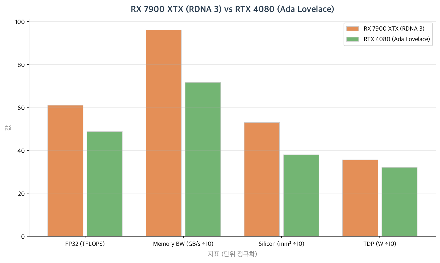
| RX 7900 XTX (RDNA 3) | RTX 4080 (Ada) | RTX 4090 (Ada) | |
|---|---|---|---|
| Process | GCD N5 / MCD N6 | Monolithic 4nm | Monolithic 4nm |
| Die | Chiplet (GCD 304 mm² + 6 MCD) | AD103 (379 mm²) | AD102 (609 mm²) |
| Shaders | 6,144 SP | 9,728 CUDA | 16,384 CUDA |
| FP32 (peak) | ~61 TFLOPS | ~48.7 TFLOPS | ~82.6 TFLOPS |
| Memory interface | GDDR6 384-bit | GDDR6X 256-bit | GDDR6X 384-bit |
| Memory bandwidth | 960 GB/s | 716.8 GB/s | 1,008 GB/s |
| VRAM | 24 GB | 16 GB | 24 GB |
| RT generation | 2nd | 3rd | 3rd |
| Frame generation | FSR 3 (SW) | DLSS 3 (HW OFA) | DLSS 3 |
| TBP | 355 W | 320 W | 450 W |
| Launch price | $999 | $1,199 | $1,599 |
Domain Breakdown
Rasterization
RX 7900 XTX matches the RTX 4080 in 4K rasterization and leads in some titles. Its memory bandwidth (960 vs. 717 GB/s) and 24 GB VRAM favor high resolutions. Its $999 price also undercut the $1,199 RTX 4080.
Ray Tracing
Ada’s 3rd-gen RT Core introduced SER (Shader Execution Reordering) and OMM (Opacity Micromap), sharply raising RT efficiency. RDNA 3’s 2nd-gen Ray Accelerator, despite its intra-generation gains, could not close the gap. In RT-enabled games the RX 7900 XTX landed around RTX 3090 Ti level, behind the RTX 4080.
Frame Generation and Upscaling
Ada introduced DLSS 3 Frame Generation, synthesizing intermediate frames using the Optical Flow Accelerator (OFA), an Ada-exclusive hardware block. It is unavailable on RDNA 3.
AMD responded with FSR 3 Fluid Motion Frames (2023): software-based frame generation that runs without dedicated hardware, working on older GPUs and NVIDIA GPUs alike. Image quality and latency consistency fell short of DLSS 3.
Power Efficiency
Ada’s 4nm monolithic design led on power efficiency. RDNA 3 trailed on performance-per-watt due to inter-chiplet communication overhead and a relatively less efficient node.
Software
The FSR Lineage
| Version | Method | Release |
|---|---|---|
| FSR 1 | Spatial upscaling | 2021 |
| FSR 2 | Temporal upscaling | 2022 |
| FSR 3 | Temporal upscaling + Fluid Motion Frames (frame gen) | 2023 |
FSR 3 answers DLSS 3’s frame generation. Unlike DLSS, every FSR version is hardware-agnostic open source and runs on NVIDIA GPUs too.
ROCm
With RDNA 3, the RX 7900 XTX entered the officially supported list for some ROCm workloads. WMMA lets consumer cards accelerate ML inference. HPC and large-scale training still center on the CDNA line.
Summary
| Item | Change vs. RDNA 2 |
|---|---|
| Die config | Monolithic → Chiplet (GCD N5 + 6 MCD N6) |
| Shaders | 1 instr/clock → Dual-Issue (conditional 2) |
| Matrix acceleration | None → WMMA (AI Accelerator) |
| Ray Accelerator | 1st-gen → 2nd-gen (~1.5×) |
| Clock | Single → front-end/shader decoupled |
| AV1 | Decode only → Encode/decode |
| DisplayPort | 1.4 → 2.1 |
| Max CUs (flagship) | 80 → 96 |
| VRAM (flagship) | 16 GB → 24 GB |
| RX 7900 XTX (RDNA 3) | RTX 4080 (Ada) | |
|---|---|---|
| FP32 peak | ~61 TFLOPS | ~48.7 TFLOPS |
| Memory BW | 960 GB/s | 716.8 GB/s |
| Raster 4K | Comparable–ahead | Baseline |
| Ray tracing | 2nd-gen, behind | 3rd-gen, ahead |
| Frame generation | FSR 3 (SW) | DLSS 3 (HW) |
| Power efficiency | Behind | Ahead |
| Launch price | $999 | $1,199 |
RDNA 3 changed GPU manufacturing economics with chiplets, splitting logic from cache/IO by process node to save costly 5nm area. Dual-Issue and WMMA raised compute density. But against Ada’s 3rd-gen RT Cores and DLSS 3, the ray tracing and frame-generation gaps remained, and chiplet overhead left it behind on power efficiency.
Next: RDNA 4 — Navi 48, 3rd-gen Ray Accelerator, FSR 4 ML upscaling