Series Roadmap
| # | Topic |
|---|---|
| 1 | The Origins of GPU and the Birth of SIMT — Tesla, Fermi |
| 2 | Kepler and Maxwell — The Pursuit of Efficiency |
| 3 | Pascal — 16nm, HBM2, NVLink |
| 4 | Volta — Tensor Cores and Independent Thread Scheduling |
| 5 | Turing — RT Cores and 2nd-Gen Tensor Cores |
| 6 | Ampere — Sparsity Acceleration and MIG |
| 7 | Hopper — Transformer Engine and FP8 |
| 8 | GPU Memory Systems and Optimization |
After Turing
Turing brought Tensor Cores and RT Cores to consumer GPUs, but the datacenter continued running V100. Between 2018 and 2020, large language model research expanded dramatically — GPT-2 (2019) and GPT-3 (2020) demanded training infrastructure at a new scale.
Simultaneously, model compression research matured. Experiments demonstrated that zeroing a substantial fraction of model weights — sparsity — caused minimal accuracy degradation. If hardware could accelerate sparse computation directly, inference throughput would double without increasing the die area or power budget.
Ampere (2020) attacked on three fronts: 3rd-generation Tensor Cores with 2:4 structured sparsity and two new precision formats (TF32, BF16), MIG (Multi-Instance GPU) for hardware-level A100 partitioning, and cp.async for software-pipelined memory access.
Die Specifications: Two Distinct Dies
Ampere splits into two distinct silicon products — one for HPC/datacenter, one for consumers.
| Turing TU102 | Ampere GA100 (A100) | Ampere GA102 (RTX 30xx) | |
|---|---|---|---|
| Process | TSMC 12nm | TSMC 7nm | Samsung 8nm |
| Transistors | 18.6B | 54.2B | 28.3B |
| Die Area | 754mm² | 826mm² | 628mm² |
| Full-die SMs | 72 | 128 (A100: 108 active) | 84 (RTX 3090: 82 active) |
| FP32 / SM | 64 | 64 | 128 |
| FP64 / SM | none | 32 | 1 (symbolic) |
| Tensor Core gen | 2nd | 3rd | 3rd |
| Representative | RTX 2080 Ti | A100 SXM4 | RTX 3090 |
| Target | Consumer/inference | HPC/large-scale AI | Consumer/gaming/AI |
GA100 moves to TSMC 7nm for transistor density. GA102 uses Samsung 8nm — a yield and cost trade-off for a consumer product. The same bifurcation seen in Pascal (GP100 vs GP102) and Turing (T4 vs TU102) repeats in Ampere.
3rd-Generation Tensor Cores
TF32: Free Speedup
TF32 (TensorFloat-32) is a new 19-bit format introduced in Ampere.
FP32 (32-bit):  sign 1 | exponent 8 | mantissa 23
TF32 (19-bit):  sign 1 | exponent 8 | mantissa 10  ← same range as FP32
FP16 (16-bit):  sign 1 | exponent 5 | mantissa 10
BF16 (16-bit):  sign 1 | exponent 8 | mantissa  7
TF32 preserves FP32’s 8-bit exponent — no overflow or underflow — while truncating the mantissa to 10 bits (FP16-level precision). cuBLAS and cuDNN use TF32 by default for Tensor Core GEMM on A100. Existing FP32 training code requires no changes to benefit from TF32 acceleration.
# Disable TF32 for precision validation
NVIDIA_TF32_OVERRIDE=0 python train.py
BF16 Tensor Cores
BF16 (Brain Float 16) — proposed by Google Brain — keeps FP32’s 8-bit exponent, eliminating the overflow risk that makes FP16 problematic for training gradient distributions with wide dynamic range. Turing processed BF16 in software on CUDA Cores. Ampere integrates BF16 directly into Tensor Core hardware.
FP64 Tensor Cores (A100 Only)
GA100 introduces FP64 Tensor Cores — the first time a GEMM unit handles double-precision matrix multiply in hardware. This delivers 2× the FP64 throughput of CUDA Cores alone.
| Precision | A100 SXM4 | V100 SXM2 |
|---|---|---|
| FP64 CUDA Core | 9.7 TFLOPS | 7.8 TFLOPS |
| FP64 Tensor Core | 19.5 TFLOPS | — |
The primary targets: scientific simulation, climate modeling, and HPC workloads that require full double-precision accuracy throughout.
2:4 Structured Sparsity
The most distinctive addition to 3rd-gen Tensor Cores is 2:4 structured sparsity. In every group of 4 consecutive values, exactly 2 must be zero. The Tensor Core hardware recognizes this pattern and skips zero multiplications.
Dense weight row (8 values):
  [0.3, 0.0, -0.5, 0.0,  0.8, 0.0, 0.2, 0.0]
       ↑         ↑             ↑        ↑   (forced to 0)

2:4 compressed storage:
  values:  [0.3, -0.5,  0.8,  0.2]           (50% compression)
  indices: [ 0,   2,    0,    2 ]             (2-bit positions within each group of 4)
During inference, the Sparse Tensor Core loads compressed values and their indices, reconstructs the sparse multiplication pattern, and produces identical outputs to the dense computation — at 2× throughput.
Sparsity workflow:
Training:
  Standard FP16/BF16 training
    → NVIDIA ASP library prunes to 2:4 pattern
    → Fine-tuning restores accuracy

Inference:
  Load compressed weights
    → Sparse Tensor Core generates dense output
    → 2× throughput vs dense
Published results show that 2:4 sparsity applied to ResNet-50, BERT, and GPT-class models produces accuracy degradation under 0.5%.
Throughput Comparison
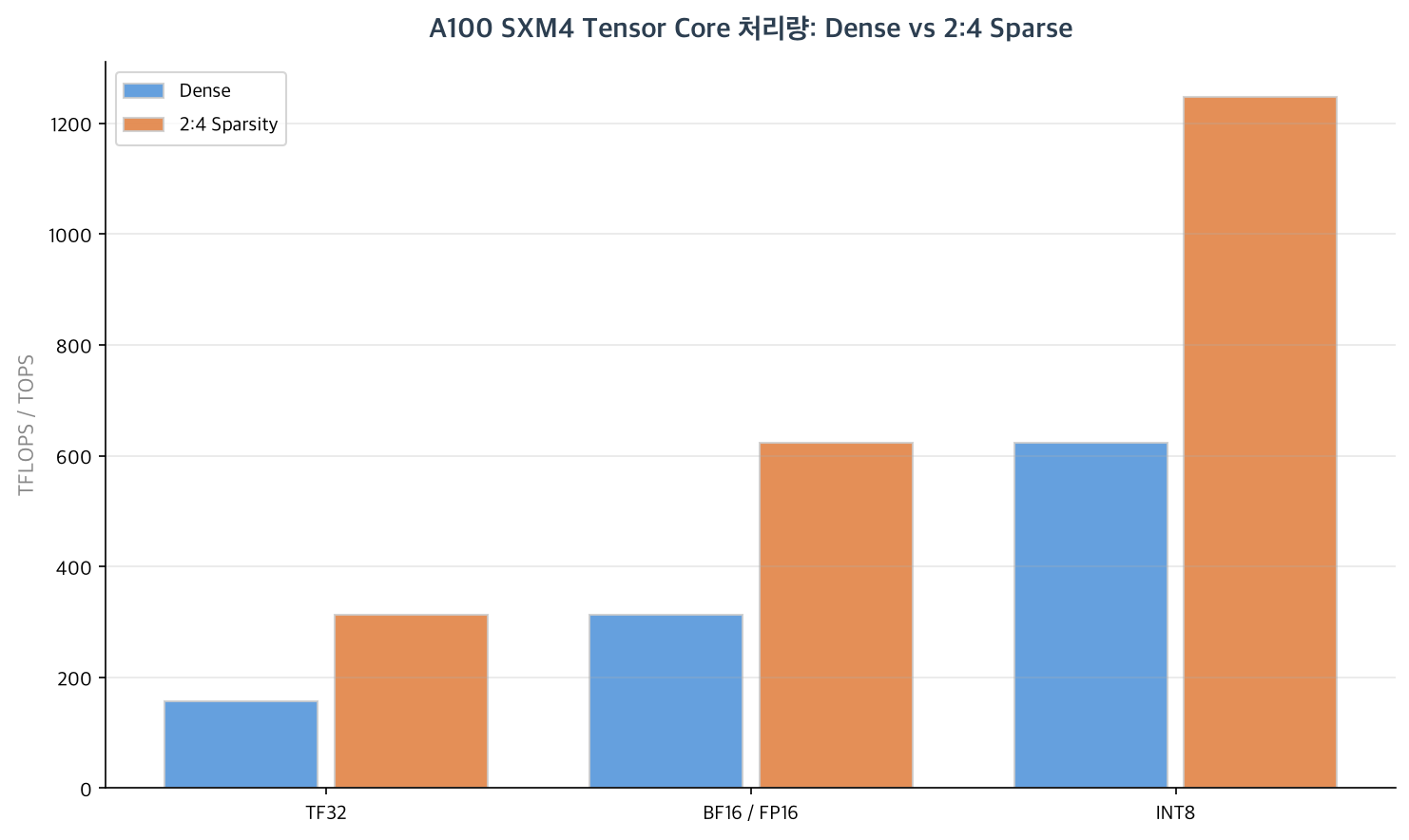
| Precision | Turing RTX 2080 Ti | A100 Dense | A100 2:4 Sparse |
|---|---|---|---|
| FP16 TC | 107.9 TFLOPS | 312 TFLOPS | 624 TFLOPS |
| BF16 TC | — | 312 TFLOPS | 624 TFLOPS |
| TF32 TC | — | 156 TFLOPS | 312 TFLOPS |
| INT8 TC | 215 TOPS | 624 TOPS | 1,248 TOPS |
| FP64 TC | — | 19.5 TFLOPS | — |
Ampere SM Structure
GA100 vs GA102 — Different Microarchitectures
Despite sharing the same Tensor Core generation, the two Ampere dies have distinct SM configurations:
GA100 Sub-core (A100)                 GA102 Sub-core (RTX 3090)
────────────────────────────          ───────────────────────────────
Warp Scheduler                        Warp Scheduler
Dispatch Unit ×2                      Dispatch Unit ×2
16 FP32           (standard)          16 FP32           (standard)
 8 FP64           (HPC)               16 FP32/INT32     ← dual-mode (new)
16 INT32          (separate)          [no FP64]
 1 TC (3rd gen)                        1 TC (3rd gen)
 8 LD/ST   4 SFU                       8 LD/ST   4 SFU

Per SM (4 sub-cores):                 Per SM (4 sub-cores):
  64 FP32 + 32 FP64 + 64 INT32          128 FP32 (+ optional INT32) + negligible FP64
GA102’s key change: the INT32 pipeline can also execute FP32 instructions, doubling FP32 throughput from 64 to 128 per SM compared to Turing TU102. FP32 and INT32 cannot be issued simultaneously from the dual-mode units — per cycle, all 128 FP32 slots are available for FP32 only.
Architecture Comparison
| Feature | Volta GV100 | Turing TU102 | Ampere GA100 | Ampere GA102 |
|---|---|---|---|---|
| FP32 / SM | 64 | 64 | 64 | 128 |
| FP64 / SM | 32 | none | 32 | 1 |
| TC generation | 1st | 2nd | 3rd | 3rd |
| TC precision | FP16 | FP16/INT8/INT4 | +TF32/BF16/FP64 TC | +TF32/BF16 |
| 2:4 Sparsity | none | none | yes (2× throughput) | yes |
| RT Core | none | 1st gen | none (datacenter) | 2nd gen |
| Unified L1+Shared | 128KB | 96KB | 192KB | 128KB |
| Max Shared Memory | 96KB | 64KB | 164KB | 100KB |
| Register file / SM | 256 KB | 256 KB | 256 KB | 256 KB |
| Max warps / SM | 64 | 32 | 64 | 48 |
| Max blocks / SM | 32 | 16 | 32 | 16 |
GA100 expands the unified L1/Shared to 192KB — critical for fitting larger GEMM tiles in shared memory and reducing global memory round-trips.
GA100 (A100) has no RT Core — it is a datacenter accelerator with no graphics functionality. GA102 (RTX 30-series) carries 2nd-gen RT Cores with higher BVH throughput than Turing’s 1st gen. GA100’s maximum occupancy matches GV100 at 64 warps/SM; GA102 sits between the two at 48 warps/SM.
MIG: Multi-Instance GPU
MIG is an A100-exclusive feature that partitions a single physical GPU into up to 7 isolated GPU instances in hardware — not time-sharing.
A100 SXM4 (108 SMs total)
┌──────────────────────────────────────────────────────────────┐
│  GPC 0 (14 SM) │ GPC 1 (14 SM) │ ... │ GPC 7 (14 SM)       │
│  L2 slice      │ L2 slice      │     │ L2 slice             │
│  HBM partition │ HBM partition │     │ HBM partition        │
└──────────────────────────────────────────────────────────────┘

7 MIG instances (each 1/7 A100):
  ┌──────┐ ┌──────┐ ┌──────┐ ┌──────┐ ┌──────┐ ┌──────┐ ┌──────┐
  │ 14SM │ │ 14SM │ │ 14SM │ │ 14SM │ │ 14SM │ │ 14SM │ │ 14SM │
  │  5GB │ │  5GB │ │  5GB │ │  5GB │ │  5GB │ │  5GB │ │  5GB │
  └──────┘ └──────┘ └──────┘ └──────┘ └──────┘ └──────┘ └──────┘
  Each instance: dedicated SM set + private L2 slice + guaranteed HBM bandwidth
MIG isolation guarantees:
- SMs: each instance uses only its allocated SMs — no cross-instance SM sharing
- L2 cache: partitioned into slices, eliminating cache interference
- Memory bandwidth: HBM2e bandwidth partitioned per instance
- Error containment: a fault in one instance does not affect others
Available MIG instance sizes (A100 40GB):
| Profile | SMs | VRAM | Max Instances |
|---|---|---|---|
| 1g.5gb | 14 | 5 GB | 7 |
| 2g.10gb | 28 | 10 GB | 3 |
| 3g.20gb | 42 | 20 GB | 2 |
| 4g.20gb | 56 | 20 GB | 1 |
| 7g.40gb | 98 | 40 GB | 1 (full GPU) |
Cloud providers use MIG to serve multiple tenants from a single A100, or to run many small inference workloads concurrently with guaranteed resource isolation.
NVLink 3.0 and Memory
NVLink 3.0
| Volta NVLink 2.0 | Ampere NVLink 3.0 | |
|---|---|---|
| Links per A100 | 6 | 12 |
| Bandwidth per link | 25 GB/s bidirectional | 25 GB/s bidirectional |
| Total per GPU | 300 GB/s | 600 GB/s |
DGX A100 nodes connect 8 A100s via NVLink 3.0 and NVSwitch 2.0. NVSwitch 2.0 provides 7.2 Tb/s non-blocking switch bandwidth, enabling AllReduce at near-memory-bandwidth speeds.
HBM2e and GDDR6X
| Product | Memory | Bandwidth | VRAM |
|---|---|---|---|
| A100 SXM4 80GB | HBM2e | 2,000 GB/s | 80 GB |
| A100 SXM4 40GB | HBM2e | 1,555 GB/s | 40 GB |
| RTX 3090 | GDDR6X | 936 GB/s | 24 GB |
| RTX 3080 | GDDR6X | 760 GB/s | 10 GB |
A100’s 2 TB/s is 2.2× V100’s 900 GB/s. GDDR6X achieves its bandwidth through PAM4 (Pulse Amplitude Modulation 4-level) signaling, doubling data per clock over standard GDDR6.
L2 Cache Partitioning
| Product | L2 Cache | Partition Structure |
|---|---|---|
| V100 (Volta) | 6 MB | single |
| RTX 2080 Ti (Turing) | 6 MB | single |
| A100 (GA100) | 40 MB | 2 × 20 MB (physically split) |
| RTX 3090 (GA102) | 6 MB | single |
A100’s 40 MB L2 is 6.7× V100’s — but the structure changed, not just the size. The GA100 die splits the L2 into two physically separate 20 MB partitions, each co-located with half the SM array. SMs primarily access their local partition at low latency; cross-partition access routes through an internal crossbar and incurs additional cycles.
This topology has two consequences:
Non-uniform L2 latency: data accessed by SMs on the far side of the crossbar pays extra cycles. Algorithms with high SM-to-data locality benefit; those that scatter data randomly across all SMs see uneven cache behavior.
MIG alignment: MIG instances are assigned to contiguous SM blocks that share a single L2 partition slice. Cross-instance L2 interference is eliminated at the hardware level — each instance’s L2 allocation is physically separate.
Ampere also introduced explicit L2 residency control APIs:
// Reserve 20 MB of L2 as a persistent region
cudaDeviceSetLimit(cudaLimitPersistingL2CacheSize, 20ULL * 1024 * 1024);

// Pin a weight buffer in L2 across kernel launches
cudaStreamAttrValue attr = {};
attr.accessPolicyWindow.base_ptr  = (void*)weight_ptr;
attr.accessPolicyWindow.num_bytes = weight_size;
attr.accessPolicyWindow.hitRatio  = 1.0f;
attr.accessPolicyWindow.hitProp   = cudaAccessPropertyPersisting;  // pin in L2
attr.accessPolicyWindow.missProp  = cudaAccessPropertyStreaming;    // bypass on miss
cudaStreamSetAttribute(stream, cudaStreamAttributeAccessPolicyWindow, &attr);
Data marked cudaAccessPropertyPersisting survives across kernel launch boundaries in L2. Repeatedly accessed buffers (weight matrices, embedding tables) can be pinned there to eliminate repeated HBM fetches. cudaAccessPropertyStreaming ensures one-time data bypasses L2 without polluting it.
cp.async: Asynchronous Memory Copy
Ampere introduces the cp.async PTX instruction: a direct copy from global memory to shared memory that bypasses the register file entirely.
Pre-Ampere (register-staged):         Ampere cp.async (direct):
Global → register → Shared Memory     Global ──────────→ Shared Memory
(register pressure, blocking)         (no registers, non-blocking)
cp.async is non-blocking — the warp issues the copy and immediately proceeds. Explicit pipeline commit/wait APIs synchronize producer and consumer stages:
#include <cuda/pipeline>

__global__ void tiled_matmul(float *A, float *B, float *C, int N) {
    __shared__ float smA[2][TILE][TILE];
    __shared__ float smB[2][TILE][TILE];

    auto pipe = cuda::make_pipeline();
    int stage = 0;

    // Prefetch first tile
    cuda::memcpy_async(smA[stage], A + ..., sizeof(smA[0]), pipe);
    cuda::memcpy_async(smB[stage], B + ..., sizeof(smB[0]), pipe);
    pipe.producer_commit();

    for (int tile = 0; tile < N / TILE; tile++) {
        int next = 1 - stage;
        // Overlap: prefetch next tile while computing current
        cuda::memcpy_async(smA[next], A + ..., sizeof(smA[0]), pipe);
        cuda::memcpy_async(smB[next], B + ..., sizeof(smB[0]), pipe);
        pipe.producer_commit();

        pipe.consumer_wait();   // wait for current tile to be ready
        __syncthreads();

        wmma::mma_sync(c_frag, a_frag, b_frag, c_frag);  // compute

        pipe.consumer_release();
        stage = next;
    }
}
CUTLASS 3.x and internal cuBLAS kernels adopt this double-buffered pipeline extensively. Memory latency and Tensor Core compute overlap, reducing SM idle time.
Scheduling: Continuation
Ampere (CC 8.0/8.6) inherits Volta’s per-thread Program Counter and call stack without modification. __syncwarp() remains the intra-warp synchronization barrier.
The cp.async pipeline introduces explicit producer-consumer synchronization as an architectural primitive. The hardware tracks outstanding async copies per pipeline; consumer_wait() stalls the warp until committed copies resolve. This is separate from warp-level scheduling — async copies proceed while the warp executes other instructions, but the warp cannot safely read the destination before consumer_wait().
CUDA 11 and Software
CUDA 11.0 (2020)
CUDA 11.0 is the first release with GA100 support. Key additions:
cp.async/cuda::pipeline— asynchronous shared memory copy API- TF32, BF16 WMMA fragment types
- MIG management via
nvidia-smi migcommands and CUDA device enumeration cooperative_groups::memcpy_async()— group-scoped async copy
DLSS 2.0
DLSS 2.0 shipped alongside Ampere but also runs on Turing Tensor Cores. The architectural shift: a single generalized temporal upscaler model replaces per-game trained models. Motion vectors and accumulated temporal data drive the upscaling network. The inference step executes on Tensor Cores in BF16 or INT8.
A100 and Large Language Models
The A100 SXM4 80GB was the workhorse for GPT-3-scale training. FP16 storage for a 175B parameter model requires approximately 350 GB — beyond any single GPU. Tensor parallelism and pipeline parallelism distribute the model across 8 A100s in a DGX node or across multiple nodes. NVLink 3.0’s 600 GB/s per GPU supports the AllReduce and activation transfers at the scale this requires.
Interconnect and External Channels
PCIe Host Interface
Ampere was NVIDIA’s first architecture with PCIe 4.0 x16 — 32 GB/s unidirectional, double PCIe 3.0.
| Product | PCIe Generation | Unidirectional BW |
|---|---|---|
| A100 PCIe | PCIe 4.0 x16 | 32 GB/s |
| RTX 3090 (GA102) | PCIe 4.0 x16 | 32 GB/s |
| RTX 2080 Ti (Turing, reference) | PCIe 3.0 x16 | 16 GB/s |
NVENC / NVDEC
| A100 (GA100) | RTX 3090 (GA102) | |
|---|---|---|
| NVENC generation | None | 8th gen |
| Encode codecs | — | H.264, HEVC, AV1 encode — first ever |
| NVDEC generation | None | 5th gen |
| Decode codecs | — | H.264, HEVC, VP9, AV1 |
| Display outputs | None | Yes |
GA102 (RTX 30-series) is the first NVIDIA generation with hardware AV1 encode. A100 omits NVENC, NVDEC, and display outputs entirely.
Display Outputs (consumer reference cards)
| Product | DP | HDMI |
|---|---|---|
| RTX 3090 (GA102) | 1.4a ×3 | 2.1 ×1 |
HDMI 2.1 supports 4K@120Hz and 8K@60Hz.
Summary
| Turing TU102 | Ampere GA100 (A100) | Ampere GA102 (RTX 3090) | |
|---|---|---|---|
| Process | 12nm | TSMC 7nm | Samsung 8nm |
| FP32 / SM | 64 | 64 | 128 |
| FP64 TC | none | 19.5 TFLOPS | none |
| TC precision | FP16/INT8/INT4 | +TF32/BF16/FP64 TC | +TF32/BF16 |
| 2:4 Sparsity | none | yes (2× throughput) | yes |
| RT Core | 1st gen | none | 2nd gen |
| PCIe | 3.0 x16 | 4.0 x16 | 4.0 x16 |
| NVENC | 7th gen | None | 8th gen (AV1) |
| MIG | none | up to 7 instances | none |
| Memory | GDDR6 616 GB/s | HBM2e 2 TB/s, 40MB L2 | GDDR6X 936 GB/s |
| NVLink | none | NVLink 3.0 (600 GB/s) | none |
| cp.async | none | yes | yes |
Ampere bifurcated cleanly. GA100 — TSMC 7nm, FP64 TC, MIG, NVLink 3.0, 40 MB L2, 2 TB/s HBM2e — addressed large-scale AI training and HPC simultaneously. GA102 — Samsung 8nm, 128 FP32/SM, 2:4 sparsity — doubled consumer FP32 throughput and brought sparse inference acceleration to gaming GPUs. The 2:4 structured sparsity mechanism established in Ampere carries forward through Hopper and Blackwell as a standard TC acceleration path.
The next post covers GPU memory systems: the register file, shared memory, the L1/L2 hierarchy, and DRAM, with optimization techniques that apply across all the architectures covered in this series.
References
- NVIDIA. NVIDIA A100 GPU Architecture Whitepaper, 2020. PDF
- NVIDIA. NVIDIA Ampere Architecture In-Depth. NVIDIA Developer Blog, 2020. Link
- NVIDIA. Exploiting NVIDIA Ampere Structured Sparsity with cuSPARSELt. NVIDIA Developer Blog, 2021.
- NVIDIA. New Features in CUDA 11.1. NVIDIA Developer Blog, 2020.
- NVIDIA. Multi-Instance GPU User Guide. NVIDIA Documentation.
- NVIDIA. CUDA C++ Programming Guide: Asynchronous Data Copies. NVIDIA Documentation.