Series Roadmap
| # | Topic |
|---|---|
| 1 | The Origins of GPU and the Birth of SIMT — Tesla, Fermi |
| 2 | Kepler and Maxwell — The Pursuit of Efficiency |
| 3 | Pascal — 16nm, HBM2, NVLink |
| 4 | Volta — Tensor Cores and Independent Thread Scheduling |
| 5 | Turing — RT Cores and 2nd-Gen Tensor Cores |
| 6 | Ampere — Sparsity Acceleration and MIG |
| 7 | Hopper — Transformer Engine and FP8 |
| 8 | Ada Lovelace — 3rd-Gen RT Cores and 96MB L2 |
| 9 | Blackwell — FP4 Tensor Cores and Multi-Die Design |
| 10 | GPU Memory Systems and Optimization |
After Ampere
A100 became the standard platform for large language model training. GPT-3 (175B parameters) required hundreds of A100s running for weeks. As models grew, the bottleneck shifted. Ampere’s BF16 Tensor Cores accelerated GEMM well, but there was no path to lower precision without sacrificing training accuracy. INT8 worked for inference but its integer-only semantics and limited dynamic range made it unsuitable for gradient computation.
The access pattern of Transformer workloads also exposed a structural constraint. Attention computation requires data exchange between tiles across different SMs within a GPC. Under Ampere, this required routing through L2 — hundreds of cycles of latency each way.
Hopper (2022) addressed both directly. The Transformer Engine and FP8 hardware broke the precision barrier for training. Thread Block Clusters and Distributed Shared Memory eliminated the L2 roundtrip for intra-GPC SM communication.
Die Specifications
| Ampere GA100 (A100) | Hopper GH100 (H100) | |
|---|---|---|
| Process | TSMC 7nm | TSMC 4nm (N4) |
| Transistors | 54.2B | 80B |
| Die Area | 826mm² | 814mm² |
| Full-die SMs | 132 | 144 |
| Active SMs | 108 (A100) | 132 (H100 SXM5) |
| FP32 / SM | 64 | 128 |
| FP64 / SM | 32 | 64 |
| TC generation | 3rd | 4th |
| L2 Cache | 40 MB (2 × 20MB partitions) | 50 MB (2 partitions) |
| Representative | A100 SXM4 80GB | H100 SXM5 80GB |
The 4nm N4 process increases transistor count from 54.2B to 80B within nearly the same die footprint. Both FP32 and FP64 CUDA Core counts double per SM relative to A100.
4th-Generation Tensor Cores and FP8
FP8 Format
FP8 is an 8-bit floating-point format introduced in Hopper. Two variants:
FP32  (32-bit): sign 1 | exponent 8 | mantissa 23
BF16  (16-bit): sign 1 | exponent 8 | mantissa  7
FP16  (16-bit): sign 1 | exponent 5 | mantissa 10
TF32  (19-bit): sign 1 | exponent 8 | mantissa 10

FP8 E4M3 ( 8-bit): sign 1 | exp 4 | mantissa 3  ← forward pass activations
FP8 E5M2 ( 8-bit): sign 1 | exp 5 | mantissa 2  ← backward pass gradients
E4M3’s 3-bit mantissa gives lower precision but sufficient exponent range for forward-pass activations and weights. E5M2 reserves one extra exponent bit, widening the dynamic range needed for gradient distributions in backpropagation.
4th-gen Tensor Cores perform FP8 × FP8 → FP32 matrix multiply. At the same 8-bit width as INT8, FP8 handles the floating-point distributions that arise in training — something integer arithmetic cannot.
Throughput
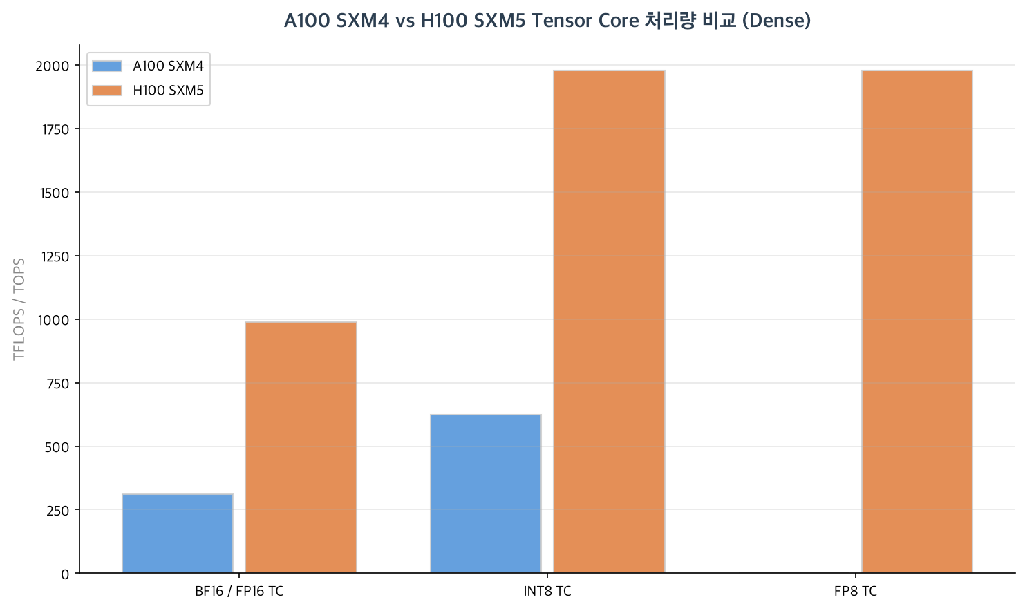
| Precision | A100 SXM4 Dense | H100 SXM5 Dense | H100 SXM5 Sparse |
|---|---|---|---|
| FP64 TC | 19.5 TFLOPS | 66.9 TFLOPS | 133.8 TFLOPS |
| TF32 TC | 156 TFLOPS | 494.7 TFLOPS | 989.4 TFLOPS |
| BF16/FP16 TC | 312 TFLOPS | 989.4 TFLOPS | 1,978.9 TFLOPS |
| FP8 TC | — | 1,978.9 TFLOPS | 3,957.8 TFLOPS |
| INT8 TC | 624 TOPS | 1,978.9 TOPS | 3,957.8 TOPS |
H100 FP8 Dense (1,978.9 TFLOPS) is 6.3× A100 BF16 Dense (312 TFLOPS). Within H100 itself, FP8 offers 2× the throughput of BF16/FP16 at the same 8-bit width as INT8.
Transformer Engine
The Training Precision Problem
FP8 training is not a drop-in replacement for BF16. Each Transformer layer has a different statistical distribution of activations and gradients. A fixed FP8 scaling factor chosen globally would cause overflow or underflow in most layers — canceling the precision gains entirely.
Per-Layer Automatic Precision Switching
The Transformer Engine is NVIDIA’s software+hardware stack that manages FP8 precision automatically at the per-layer level.
Transformer Engine layer execution:
──────────────────────────────────────────────────────────────

Input tensor (BF16/FP32)
   │
   ▼
[Compute scale factor]  ← from recent amax (max absolute value) history
   │                         scale = FP8_max / amax   (E4M3 max ≈ 448)
   ▼
[Cast: input × scale → FP8 E4M3]
   │
   ▼
[FP8 × FP8 Tensor Core GEMM]  ← 4th-gen TC, FP32 accumulation
   │          ↑
   │   [FP8 weights: pre-cast and stored in compressed form]
   ▼
[FP32 accumulation result]
   │
   ▼
[Descale: result / scale → BF16/FP32 output]
   │
   ▼
Next layer (BF16/FP32)
Scale factors are tracked per-tensor or per-channel. The history of recent amax values (configurable length) is used to predict the appropriate scale for the next forward pass. Backward pass gradients use E5M2 with their own per-tensor scale.
import transformer_engine.pytorch as te
import transformer_engine.common.recipe as recipe

fp8_recipe = recipe.DelayedScaling(
    margin=0,
    interval=1,
    fp8_format=recipe.Format.HYBRID,  # E4M3 forward, E5M2 backward
    amax_history_len=16,
    amax_compute_algo="max"
)

# Drop-in replacement for torch.nn layers
model = te.TransformerLayer(hidden_size, ffn_hidden_size, num_attention_heads)

with te.fp8_autocast(enabled=True, fp8_recipe=fp8_recipe):
    output = model(input_tensor, attention_mask)
Hopper SM Structure
Comparison with Ampere
Hopper GH100 Sub-core
───────────────────────────────
Warp Scheduler
Dispatch Unit ×2
32 FP32            (standard)
16 FP64            (HPC)
32 FP32/INT32      (dual-mode)
 1 TC (4th gen)    FP8/FP16/BF16/TF32/INT8/FP64 TC
 8 LD/ST   4 SFU

Per SM (4 sub-cores):
  128 FP32, 64 FP64, 4 TC (4th gen)
| Feature | Ampere GA100 (A100) | Hopper GH100 (H100) |
|---|---|---|
| FP32 / SM | 64 | 128 |
| FP64 / SM | 32 | 64 |
| TC generation | 3rd | 4th |
| TC precision | TF32/BF16/FP16/INT8/FP64 TC | +FP8 (E4M3, E5M2) |
| 2:4 Sparsity | yes | yes |
| RT Core | none | none (datacenter) |
| Distributed Shared Memory | none | yes |
| Unified L1+Shared | 192KB | 228KB |
| Max Shared Memory | 164KB | 228KB |
| Register file / SM | 256 KB | 256 KB |
| Max warps / SM | 64 | 64 |
| Max blocks / SM | 32 | 32 |
Both FP32 and FP64 per SM double from A100 to H100 — the 4nm process node provides the transistor density without increasing die area. GH100 supports up to 64 warps/SM, 32 blocks/SM in-flight, matching A100.
H100 (GH100) has no RT Core. RT Cores appear only in consumer-facing Turing and Ampere GA102 dies. A100 also lacks RT Cores; H100 follows the same policy — the die area is allocated to FP64 TC, Transformer Engine logic, and greater SM counts instead.
The unified L1+Shared grows to 228KB, and the full 228KB can be configured as shared memory (up to 228KB, vs A100’s max 164KB). This benefits large-tile GEMM and Flash Attention implementations that tile KV matrices into shared memory.
Thread Block Clusters and Distributed Shared Memory
The L2 Roundtrip Problem
Before Hopper, inter-SM data sharing went through L2:
Ampere and earlier:
SM 0 (Shared Memory A) ──→ L2 Cache ──→ SM 1 (Shared Memory B)
                       (hundreds of cycles roundtrip)
For Attention computation, each tile needs values from adjacent tiles processed by neighboring SMs. Under Ampere, this round-trips through 40MB L2 — fast relative to HBM, but still costly at scale.
Thread Block Cluster
A Thread Block Cluster groups up to 8 Thread Blocks within the same GPC into a cooperative unit with guaranteed co-execution and direct SM-to-SM shared memory access.
Hopper Thread Block Cluster (within one GPC):
┌──────────────────────────────────────────────────────┐
│  GPC                                                 │
│  ┌──────────┐  ┌──────────┐  ┌──────────┐           │
│  │  SM 0    │  │  SM 1    │  │  SM 2    │           │
│  │ Block 0  │  │ Block 1  │  │ Block 2  │           │
│  │ Shared ◄─┼──┼─► Shared ◄┼──┼─► Shared │           │
│  │ Memory   │  │  Memory  │  │  Memory  │           │
│  └──────────┘  └──────────┘  └──────────┘           │
│   direct SM-to-SM path (no L2 roundtrip)            │
└──────────────────────────────────────────────────────┘
The execution hierarchy gains one level:
Grid
└─ Cluster  ← new in CUDA 12 (up to 8 blocks, GPC-scoped)
   └─ Thread Block  (SM-scoped)
      └─ Warp  (32 threads)
         └─ Thread
Co-execution within a cluster is guaranteed — unlike ordinary thread blocks, which may or may not run concurrently.
// CUDA 12: Thread Block Cluster launch
cudaLaunchAttribute attr[1];
attr[0].id = cudaLaunchAttributeClusterDimension;
attr[0].val.clusterDim = {4, 1, 1};  // 4-block cluster

cudaLaunchKernelEx(&config, my_kernel, args...);

// Inside the kernel:
__global__ void my_kernel() {
    namespace cg = cooperative_groups;
    auto cluster = cg::this_cluster();

    __shared__ float smem[TILE];

    // Get pointer to a peer block's shared memory
    float *peer_smem = cluster.map_shared_rank(smem, /* peer_rank */ 1);
    cluster.sync();                      // cluster-wide barrier
    float val = peer_smem[threadIdx.x]; // direct read from peer SM's shared memory
}
Application: Flash Attention v3
Flash Attention v3 uses Thread Block Cluster to exchange KV tiles between neighboring SMs without L2. Each SM processes a slice of the attention computation; the Q tile on one SM directly reads the K/V tiles on peer SMs within the same cluster. Benchmarks show ~1.5–2× speedup over Flash Attention v2 on H100.
Warp Specialization
Hopper formalizes warp specialization as a first-class pattern. Within a single thread block, a subset of warps act as producers (issuing cp.async loads) and the remainder act as consumers (executing Tensor Core MMA). The two groups synchronize via cuda::pipeline.
__global__ void warp_specialized(float *A, float *B, float *C) {
    auto pipe = cuda::make_pipeline();
    __shared__ float smA[2][TILE][TILE];
    __shared__ float smB[2][TILE][TILE];

    if (warp_is_producer()) {
        for (int i = 0; i < tiles; i++) {
            cuda::memcpy_async(smA[i % 2], A + offset(i), size, pipe);
            cuda::memcpy_async(smB[i % 2], B + offset(i), size, pipe);
            pipe.producer_commit();
        }
    } else {
        for (int i = 0; i < tiles; i++) {
            pipe.consumer_wait();
            __syncwarp();
            wmma::mma_sync(c_frag, a_frag, b_frag, c_frag);
            pipe.consumer_release();
        }
    }
}
Producer warps overlap memory fetches with consumer warps executing Tensor Core operations — achieving near-full memory and compute utilization simultaneously.
NVLink 4.0, HBM3, and L2 Cache
NVLink 4.0
| Ampere NVLink 3.0 | Hopper NVLink 4.0 | |
|---|---|---|
| Links per GPU | 12 | 18 |
| Bandwidth per link | 25 GB/s bidirectional | 25 GB/s bidirectional |
| Total per GPU | 600 GB/s | 900 GB/s |
NVSwitch 3.0 switches provide 13.6 Tb/s per-switch non-blocking bandwidth. A DGX H100 node connects 8 H100s at full all-to-all 900 GB/s per GPU.
HBM3
| Product | Memory | Bandwidth | VRAM |
|---|---|---|---|
| A100 SXM4 80GB | HBM2e | 2,000 GB/s | 80 GB |
| H100 SXM5 80GB | HBM3 | 3,350 GB/s | 80 GB |
| H100 PCIe 80GB | HBM2e | 2,000 GB/s | 80 GB |
H100 SXM5’s HBM3 delivers 3.35 TB/s — 1.67× A100. The H100 PCIe variant retains HBM2e due to board power and form factor constraints.
L2 Cache Partitioning
The A100’s 40MB L2 and H100’s 50MB L2 are both physically divided into two separate partitions (each ~20MB for A100, ~25MB for H100). Each partition is co-located with half the SM array on the die. SMs primarily access their local partition; cross-partition traffic is routed through an internal crossbar.
This topology has two direct consequences:
-
Non-uniform L2 latency: SMs on the far side of the partition boundary pay extra cycles for cross-partition access. Data layout choices that respect partition locality improve effective cache bandwidth.
-
Persistent L2 residency (API): Ampere introduced explicit control over which data stays in L2 across kernels:
// Reserve half the L2 as a persistent region
cudaDeviceSetLimit(cudaLimitPersistingL2CacheSize, 20 * 1024 * 1024);

// Mark a data window as persisting across kernel launches
cudaStreamAttrValue attr;
attr.accessPolicyWindow.base_ptr   = (void*)weights;
attr.accessPolicyWindow.num_bytes  = weights_size;
attr.accessPolicyWindow.hitRatio   = 1.0;
attr.accessPolicyWindow.hitProp    = cudaAccessPropertyPersisting;
attr.accessPolicyWindow.missProp   = cudaAccessPropertyStreaming;
cudaStreamSetAttribute(stream, cudaStreamAttributeAccessPolicyWindow, &attr);
Frequently reused data (embedding tables, weight matrices accessed by many kernels) can be pinned in the persistent L2 region, eliminating repeated HBM fetches. This API was introduced in Ampere and carries forward into Hopper unchanged.
MIG partitioning in A100/H100 aligns with L2 partitions: each MIG instance is assigned to a contiguous block of SMs that share a single L2 partition, ensuring full L2 isolation between instances.
GH200 Grace Hopper Superchip
GH200 is NVIDIA’s first CPU+GPU integrated product. An ARM-based Grace CPU and an H100 GPU die are connected via NVLink-C2C.
GH200 Grace Hopper Superchip
┌──────────────────────────────────────────────────────────┐
│                                                          │
│   Grace CPU (ARM Neoverse V2)    H100 GPU (GH100)       │
│   ┌─────────────────────┐        ┌────────────────────┐  │
│   │ 72 Neoverse V2 cores│        │ 132 SMs (Hopper)   │  │
│   │ 96 GB LPDDR5X       │        │ 80/96 GB HBM3/3e   │  │
│   │ 512 GB/s CPU mem BW │        │ 3.35 TB/s HBM BW   │  │
│   └──────────┬──────────┘        └──────┬─────────────┘  │
│              │                          │                 │
│              └──────── NVLink-C2C ──────┘                │
│                        900 GB/s bidirectional             │
│                        (7× PCIe 5.0 x16)                 │
│                                                          │
└──────────────────────────────────────────────────────────┘
The key capability: GPU kernels can directly address CPU LPDDR5X memory through a coherent unified address space. The 96GB of LPDDR5X extends the GPU’s effective memory capacity beyond HBM.
| H100 SXM5 (discrete) | GH200 | |
|---|---|---|
| CPU-GPU interface | PCIe 5.0 x16 (~128 GB/s) | NVLink-C2C (900 GB/s) |
| CPU memory access | not directly addressable | 96 GB LPDDR5X (GPU-addressable) |
| Total addressable memory | GPU HBM only | HBM + CPU LPDDR5X |
| Address space | separate | unified |
For large-context inference workloads where KV caches exceed HBM capacity, GH200 allows the GPU to use CPU LPDDR5X as a lower-bandwidth extension without explicit cudaMemcpy.
Interconnect and External Channels
PCIe Host Interface
The H100 PCIe card is NVIDIA’s first GPU with PCIe 5.0 x16 — 64 GB/s unidirectional (2× PCIe 4.0). H100 SXM5 also uses PCIe 5.0 for host connectivity; NVLink 4.0 handles GPU-to-GPU traffic.
| Product | PCIe Generation | Unidirectional BW |
|---|---|---|
| H100 SXM5 | PCIe 5.0 x16 | 64 GB/s |
| H100 PCIe | PCIe 5.0 x16 | 64 GB/s |
| A100 (reference) | PCIe 4.0 x16 | 32 GB/s |
HBM3 Bus Width
H100 SXM5’s HBM3 spans 5 stacks × 1,024-bit = 5,120-bit total bus, delivering 3,350 GB/s peak bandwidth.
External Channels
H100 is a datacenter-only accelerator. The following are absent by design:
| Feature | Status |
|---|---|
| RT Core | None |
| NVENC | None |
| NVDEC | None |
| Display outputs | None |
Summary
| Ampere GA100 (A100) | Hopper GH100 (H100) | |
|---|---|---|
| Process | TSMC 7nm | TSMC 4nm (N4) |
| FP32 / SM | 64 | 128 |
| FP64 / SM | 32 | 64 |
| TC generation | 3rd | 4th |
| FP8 | none | E4M3 / E5M2 |
| Transformer Engine | none | yes |
| Thread Block Cluster | none | yes (up to 8 blocks) |
| Distributed Shared Memory | none | yes |
| RT Core | none | none |
| NVLink | 3.0 (600 GB/s) | 4.0 (900 GB/s) |
| PCIe | 4.0 x16 | 5.0 x16 |
| NVENC | none | none |
| Memory | HBM2e 2 TB/s, 40MB L2 | HBM3 3.35 TB/s, 50MB L2 |
| Max Shared Memory | 164KB | 228KB |
| MIG | yes (7 instances) | yes (7 instances) |
Hopper’s defining feature is the Transformer Engine and FP8. The 2× throughput gain from BF16 to FP8 (at the same 8-bit width) is accessible in training without accuracy loss — a combination that was not achievable with INT8 alone. Thread Block Clusters remove the L2 penalty from intra-GPC communication, directly benefiting Attention kernels. GH200 redefines the memory boundary between CPU and GPU, enabling inference workloads that exceed HBM capacity to remain on-GPU rather than offloading to the host.
The next post covers GPU memory systems: the register file, shared memory, the L1/L2 hierarchy, and DRAM — with optimization techniques drawn from the architectural evolution documented in this series.
References
- NVIDIA. NVIDIA Hopper GPU Architecture Whitepaper, 2022. PDF
- NVIDIA. NVIDIA H100 Tensor Core GPU Architecture In-Depth. NVIDIA Developer Blog, 2022.
- NVIDIA. NVIDIA Transformer Engine. GitHub, 2022. Link
- Shah, J. et al. FlashAttention-3: Fast and Accurate Attention with Asynchrony and Low-precision. arXiv:2407.08608, 2024.
- NVIDIA. CUDA C++ Programming Guide: Thread Block Clusters. CUDA 12 Documentation.
- NVIDIA. GH200 Grace Hopper Superchip Architecture Whitepaper, 2023.
- NVIDIA. L2 Cache Residency Control. CUDA Best Practices Guide.