Series Roadmap
| # | Topic |
|---|---|
| 1 | The Origins of GPU and the Birth of SIMT — Tesla, Fermi |
| 2 | Kepler and Maxwell — The Pursuit of Efficiency |
| 3 | Pascal — 16nm, HBM2, NVLink |
| 4 | Volta — Tensor Cores and Independent Thread Scheduling |
| 5 | Turing — RT Cores and 2nd-Gen Tensor Cores |
| 6 | Ampere — Sparsity Acceleration and MIG |
| 7 | Hopper — Transformer Engine and FP8 |
| 8 | Ada Lovelace — 3rd-Gen RT Cores and 96MB L2 |
| 9 | Blackwell — FP4 Tensor Cores and Multi-Die Design |
| 10 | GPU Memory Systems and Optimization |
After Hopper and Ada
Hopper’s FP8 Transformer Engine dramatically increased LLM training throughput. Two constraints remained.
The first was inference cost. FP8 is effective for both training and inference, but as 100B+ parameter models became standard, there was no hardware path below 8-bit precision. Software-level INT4/FP4 quantization existed but lacked direct Tensor Core support — throughput gains were limited by the mismatch between quantization format and TC hardware.
The second was HBM capacity. H100 SXM5 carries 80GB of HBM3. Models too large to fit in a single GPU required tensor-parallel multi-GPU configurations, adding communication overhead and complexity. Doubling single-accelerator capacity required either a process node change or a fundamentally different packaging approach.
Blackwell (2024) addressed both from two directions simultaneously. The datacenter GB100 used a two-die MCM to break past single-die physical constraints. The consumer GB202 combined GDDR7, PCIe 5.0, and DLSS 4 Multi-Frame Generation to redefine the consumer GPU tier.
Die Specifications
Datacenter: GB100 vs GH100
| GH100 (Hopper, H100 SXM5) | GB100 (Blackwell, B200 SXM) | |
|---|---|---|
| Process | TSMC 4nm (N4) | TSMC 4NP |
| Die configuration | Single die | 2-die MCM |
| Transistors | 80B | 208B |
| Active SMs | 132 (H100) | ~168 (B200) |
| FP32 / SM | 128 | 128 |
| TC generation | 4th | 5th |
| HBM generation | HBM3 | HBM3e |
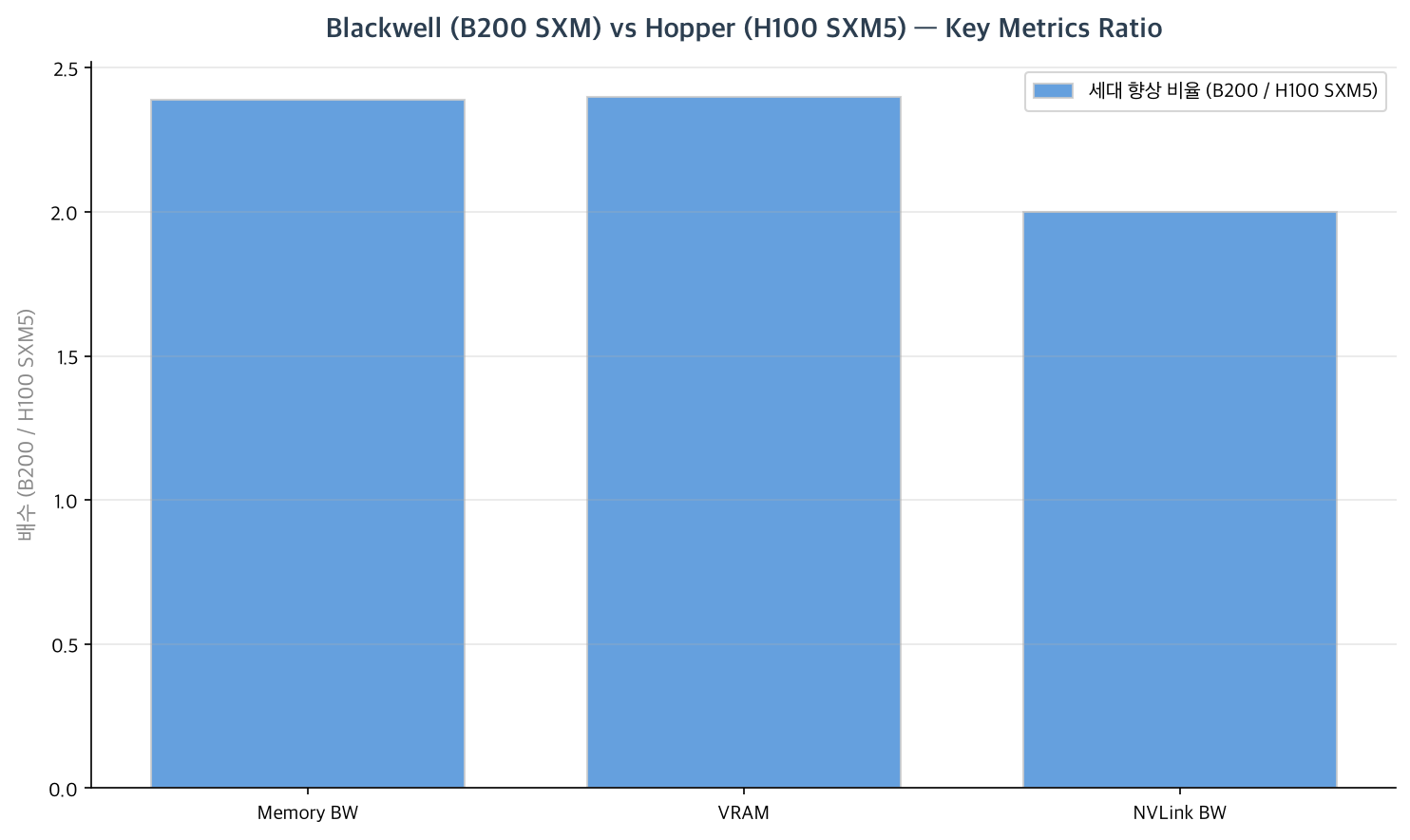
| VRAM | 80GB | 192GB |
| Memory bandwidth | 3.35 TB/s | ~8 TB/s |
| NVLink | 4.0 (900 GB/s) | 5.0 (1,800 GB/s) |
Consumer: GB202 vs AD102
| AD102 (Ada, RTX 4090) | GB202 (Blackwell, RTX 5090) | |
|---|---|---|
| Process | TSMC 4N | TSMC 4NP |
| Full-die SMs | 144 | ~170 |
| Active SMs | 128 | ~170 |
| FP32 / SM | 128 | 128 |
| TC generation | 4th | 5th |
| RT Core generation | 3rd | 4th |
| DRAM type | GDDR6X | GDDR7 |
| Memory bus | 384-bit | 512-bit |
| VRAM | 24GB | 32GB |
| Memory bandwidth | 1,008 GB/s | 1,792 GB/s |
Two-Die MCM Architecture (Datacenter GB100)
The most significant structural change in Blackwell’s datacenter tier. GB100 integrates two Blackwell dies in a single package — a Multi-Chip Module (MCM) design.
GB100 Package Layout
┌─────────────────────────────────────────────────────┐
│  Blackwell Die 0           Blackwell Die 1          │
│  (half of SMs + 4 HBM3e)  (half of SMs + 4 HBM3e) │
│                                                     │
│          ◄──── NV-HBI ────►                         │
│         (inter-die interconnect)                    │
│                                                     │
│  ┌──────────────────────────────────────────────┐   │
│  │  HBM3e ×4            HBM3e ×4               │   │
│  │  (96GB)              (96GB)                 │   │
│  └──────────────────────────────────────────────┘   │
│  Total HBM3e: 192GB / 8,192-bit bus / ~8 TB/s       │
└─────────────────────────────────────────────────────┘
NV-HBI (NVIDIA High Bandwidth Interconnect) is the on-package die-to-die link. From software’s perspective, the two dies appear as a single unified GPU. CUDA kernels have no awareness of die boundaries; the memory address space is a flat 192GB.
Advantages of this design:
- Memory capacity (192GB) and bandwidth (~8 TB/s) unreachable with any single manufacturable die
- Yield: two smaller dies have higher per-unit manufacturing yield than one equivalent monolithic die
For comparison: Ada AD102 is a monolithic 76.3B-transistor die. GB100’s two-die MCM achieves 208B transistors — 2.7× more — while remaining manufacturable.
5th-Gen Tensor Cores: FP4 and MXFP8
FP4 (E2M1)
FP4 is the first 4-bit floating-point precision supported in hardware Tensor Cores, introduced in Blackwell.
FP32  (32-bit): sign 1 | exponent 8 | mantissa 23
FP16  (16-bit): sign 1 | exponent 5 | mantissa 10
FP8 E4M3 ( 8-bit): sign 1 | exp 4 | mantissa 3
FP4 E2M1 ( 4-bit): sign 1 | exp 2 | mantissa 1  ← Blackwell new
FP4 E2M1 has an extremely limited representable range — 8 non-zero values per sign. Successful FP4 quantization requires careful calibration of weight and activation distributions. MXFP4 per-block scaling (described below) is the practical mechanism that makes FP4 usable.
Throughput hierarchy:
FP32 (CUDA Cores) : baseline
FP16 TC Dense     : ~4× FP32
FP8  TC Dense     : ~8× FP32  (since Hopper)
FP4  TC Dense     : ~16× FP32 (Blackwell new)
FP4 TC delivers 2× the throughput of FP8 TC at the same hardware. For inference workloads where the model fits within FP4 accuracy requirements, the effective model capacity per accelerator doubles compared to FP8.
MXFP8 — Microscaling
Hopper’s Transformer Engine applied one scaling factor per tensor. For tensors with wide value distributions, values exceeding the FP8 representable range either saturate or underflow — introducing quantization error.
MXFP (MicroScaling Floating Point) is an Open Compute Project (OCP) standard format. It assigns a separate scaling factor to every block of 32 elements.
Hopper FP8 (per-tensor scaling):
┌────────────────────────────────┐
│  Entire tensor → one scale     │
│  Wide range → elevated error   │
└────────────────────────────────┘

Blackwell MXFP8 (per-block scaling):
┌────────┐┌────────┐┌────────┐
│ Block 0 ││ Block 1 ││ Block 2 │  ← 32 elements each
│ scale 0 ││ scale 1 ││ scale 2 │  ← independent scale per block
└────────┘└────────┘└────────┘
→ locally optimal precision across all blocks
MXFP supports FP8, FP6, and FP4 variants. Per-block scaling eliminates the need for Hopper Transformer Engine’s dynamic scale-search heuristics, making the quantization workflow more predictable. 5th-gen Tensor Cores natively support MXFP4, MXFP6, MXFP8 alongside FP8, FP16, BF16, TF32, and INT8.
SM Structure
Blackwell’s SM retains the same 4-sub-core design as Ada. The changes are TC and RT Core generations.
Blackwell SM (GB202, CC 10.0)
┌──────────────────────────────────────────────────────┐
│  Sub-core 0                  Sub-core 1              │
│  Warp Scheduler × 1          Warp Scheduler × 1      │
│  FP32 × 16 + FP32/INT32 × 16  (32 FP32 per sub-core)│
│  Tensor Core × 1 (5th gen)   Tensor Core × 1         │
│  LD/ST × 8 | SFU × 4        LD/ST × 8 | SFU × 4    │
├──────────────────────────────────────────────────────┤
│  Sub-core 2                  Sub-core 3              │
│  (identical structure)        (identical structure)   │
├──────────────────────────────────────────────────────┤
│  RT Core × 1 (4th gen, shared across the SM)         │
├──────────────────────────────────────────────────────┤
│  L1 Cache + Shared Memory   (configurable)           │
│  Register File              256KB                    │
└──────────────────────────────────────────────────────┘

Per-SM totals:
  FP32: 128 | TC: 4 (5th gen) | RT Core: 1 (4th gen)
  LD/ST: 32 | SFU: 16
Ada to Blackwell SM delta:
| AD102 (Ada, CC 8.9) | GB202 (Blackwell, CC 10.0) | |
|---|---|---|
| FP32 / SM | 128 | 128 |
| TC generation | 4th | 5th (FP4, MXFP8) |
| RT Core generation | 3rd | 4th |
| FP4 TC | None | Yes |
| LD/ST | 32 | 32 |
| Register File | 256KB | 256KB |
Consumer Innovations: DLSS 4 and Neural Rendering
DLSS 4 Multi-Frame Generation
Ada’s DLSS 3 inserted one AI-generated frame between each pair of rendered frames. Blackwell’s DLSS 4 introduces Multi-Frame Generation (MFG), inserting up to three AI frames per rendered frame.
DLSS 3 (Ada):
render → [AI×1] → render → [AI×1] → render ...
Displayed: 1 rendered + 1 AI = 2× multiplier

DLSS 4 MFG (Blackwell):
render → [AI×3] → render → [AI×3] → render ...
Displayed: 1 rendered + 3 AI = 4× multiplier
Combined with DLSS Super Resolution: rendering at 1080p, upscaling to 4K with SR, then applying 4× MFG means the GPU renders at 1080p native while the display receives 4K output at 4× the rendered frame rate. The actual 3D rendering workload is a fraction of what native 4K would require.
Higher MFG multipliers increase the fraction of AI-generated frames, which adds input latency proportionally. NVIDIA Reflex mitigates this by reducing render queue depth between game engine and driver.
Neural Shaders
A new rendering concept introduced in Blackwell. HLSL shader programs can invoke tiny neural network inference directly during shader execution, with the SM’s Tensor Cores processing the neural network layers inline.
Traditional rendering:
  Rasterize → Shader (CUDA Cores) → Output

Neural Shader (Blackwell):
  Rasterize → Shader (CUDA Cores) ─┐
                                    ├─ Tensor Cores (tiny NN inference)
                                    └─ Output
This enables shaders to evaluate complex material responses (lighting, subsurface scattering, appearance models) using neural approximations rather than analytic BRDFs, at costs proportional to the neural network size.
Neural Texture Compression
Traditional textures use block-compression formats (BC7, ASTC). Neural Texture Compression replaces the fixed block-compression decoder with a small neural decoder that runs on Tensor Cores at texture sample time. The same VRAM budget stores higher-fidelity texture data, or the same visual quality fits in less VRAM. From the API perspective the usage is identical to standard texture sampling.
Scheduling
Blackwell’s SM warp scheduling model carries forward from Ada: 4 independent warp schedulers per SM, independent thread scheduling (from Volta), and SER support (from Ada). The per-SM fundamentals are unchanged.
Interconnect and External Channels
NVLink 5.0 (Datacenter GB100)
| Generation | BW (bidirectional / GPU) | First architecture |
|---|---|---|
| NVLink 1.0 | 160 GB/s | Pascal GP100 |
| NVLink 2.0 | 300 GB/s | Volta GV100 |
| NVLink 3.0 | 600 GB/s | Ampere GA100 |
| NVLink 4.0 | 900 GB/s | Hopper GH100 |
| NVLink 5.0 | 1,800 GB/s | Blackwell GB100 |
NVLink 5.0 doubles the per-GPU bidirectional bandwidth over NVLink 4.0. In the GB200 NVL72 configuration, 72 B200 GPUs are interconnected via NVLink 5.0 switches. AllReduce communication within the 72-GPU domain travels entirely over NVLink fabric without touching PCIe or InfiniBand.
PCIe
| Architecture | PCIe | Note |
|---|---|---|
| Ada (RTX 4090) | 4.0 x16 | — |
| Hopper (H100) | 5.0 x16 | First datacenter PCIe 5.0 |
| Blackwell (RTX 5090) | 5.0 x16 | First consumer PCIe 5.0 |
Blackwell consumer GPUs upgraded from PCIe 4.0 (Ada) to PCIe 5.0 — the first consumer GPUs to do so. Hopper was the first GPU of any class with PCIe 5.0.
Memory Subsystem
| Product | DRAM | Bus | Bandwidth | Capacity |
|---|---|---|---|---|
| RTX 4090 (AD102) | GDDR6X | 384-bit | 1,008 GB/s | 24GB |
| RTX 5090 (GB202) | GDDR7 | 512-bit | 1,792 GB/s | 32GB |
| H100 SXM5 (GH100) | HBM3 | 5,120-bit | 3.35 TB/s | 80GB |
| B200 SXM (GB100) | HBM3e | 8,192-bit | ~8 TB/s | 192GB |
RTX 5090 GDDR7 bandwidth (1,792 GB/s) is 1.78× the RTX 4090 GDDR6X (1,008 GB/s).
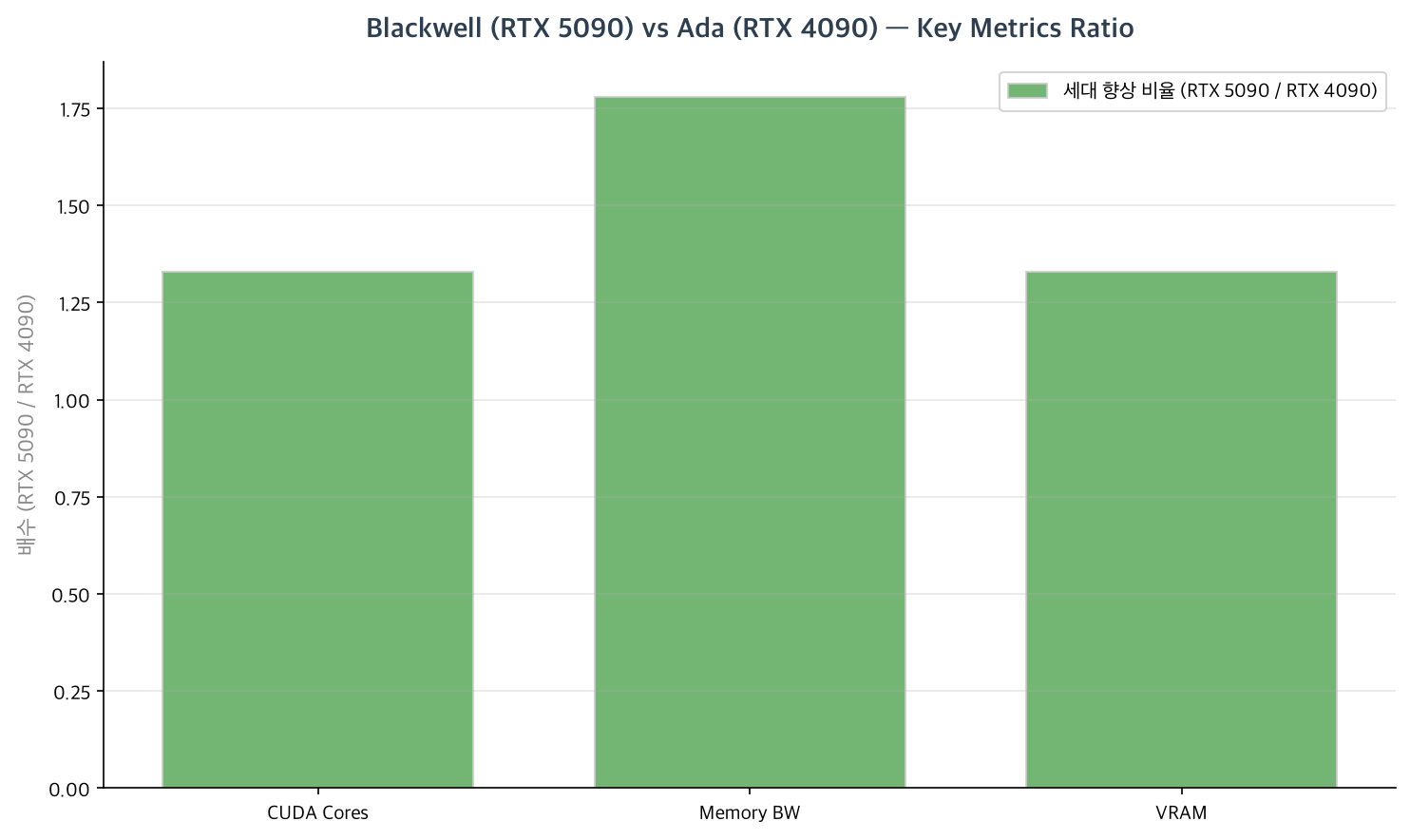
B200 SXM’s ~8 TB/s bandwidth is 2.4× H100 SXM5 (3.35 TB/s). The two-die MCM enables 8 HBM3e stacks (4 per die), where a single monolithic die could not accommodate more than 5–6 stacks.
NVENC / NVDEC and Display
| Product | NVENC count | AV1 encode | Display outputs |
|---|---|---|---|
| RTX 4090 (AD102) | 2 (dual) | Yes | DP 1.4a ×3, HDMI 2.1 ×1 |
| RTX 5090 (GB202) | 2 (dual) | Yes | DP 2.1b ×3, HDMI 2.1 ×1 |
| B200 SXM (GB100) | None | — | None |
RTX 5090 upgrades to DisplayPort 2.1b, which supports 8K@60Hz on a single cable without DSC. NVENC count remains at two.
Summary
| GH100 / AD102 | GB100 / GB202 | |
|---|---|---|
| Process | TSMC 4nm | TSMC 4NP |
| Die config | Single | 2-die MCM (GB100) |
| TC generation | 4th | 5th (FP4, MXFP8) |
| FP4 TC | None | Yes |
| RT Core generation | 3rd (Ada) | 4th |
| Memory BW | 3.35 TB/s / 1,008 GB/s | ~8 TB/s / 1,792 GB/s |
| VRAM | 80GB / 24GB | 192GB / 32GB |
| NVLink | 4.0 (900 GB/s) | 5.0 (1,800 GB/s) |
| PCIe (consumer) | 4.0 x16 (Ada) | 5.0 x16 |
| DLSS Frame Gen | ×1 (DLSS 3) | ×3 (DLSS 4 MFG) |
| Neural Shaders | None | Yes |
Blackwell broke past the single-die physical limit on the datacenter side with two-die MCM, and pushed FP4 Tensor Core inference into hardware — cutting per-token inference cost in half relative to FP8. On the consumer side, GDDR7, PCIe 5.0, and DLSS 4 MFG (3×) deliver across-the-board generational gains over Ada. The integration of Tensor Cores into the rendering pipeline itself — Neural Shaders, Neural Texture Compression — marks the beginning of a structural shift in how GPU compute is used within traditional graphics workloads.
References
- NVIDIA. NVIDIA Blackwell Architecture Technical Brief. 2024.
- NVIDIA. NVIDIA GB200 NVL72 Platform Overview. 2024.
- NVIDIA. GeForce RTX 5090 Product Specifications. 2025.
- NVIDIA. DLSS 4 with Multi Frame Generation Technical Overview. 2025.
- OCP. MX Microscaling Formats Specification. Open Compute Project, 2023.