Series Roadmap
| # | Topic |
|---|---|
| 1 | The Origins of GPU and the Birth of SIMT — Tesla, Fermi |
| 2 | Kepler and Maxwell — The Pursuit of Efficiency |
| 3 | Pascal — 16nm, HBM2, NVLink |
| 4 | Volta — Tensor Cores and Independent Thread Scheduling |
| 5 | Turing — RT Cores and 2nd-Gen Tensor Cores |
| 6 | Ampere — Sparsity Acceleration and MIG |
| 7 | Hopper — Transformer Engine and FP8 |
| 8 | Ada Lovelace — 3rd-Gen RT Cores and 96MB L2 |
| 9 | Blackwell — FP4 Tensor Cores and Multi-Die Design |
| 10 | GPU Memory Systems and Optimization |
After Ampere
GA102 (RTX 30-series) brought real-time ray tracing to the mainstream with 2nd-gen RT Cores. Two bottlenecks remained.
The first was transparent geometry. Scenes with glass, foliage, and alpha-textured surfaces required an AnyHit shader — running on a SM — every time a ray hit a potentially transparent triangle during BVH traversal. This stalled RT Core throughput waiting for the SM to return a hit/miss decision.
The second was L2 cache capacity. GA102 had 6MB of L2. Ray tracing BVH traversal is inherently non-uniform: each ray takes a different path through the BVH, making cache reuse low. 6MB was too small to hold even the upper layers of a complex scene’s BVH.
Ada Lovelace (AD102, September 2022) attacked both with 3rd-gen RT Cores, 96MB L2, and 4th-gen Tensor Cores (FP8).
Die Specifications
| GA102 (Ampere, RTX 3090) | AD102 (Ada, RTX 4090) | |
|---|---|---|
| Process | Samsung 8nm | TSMC 4N (4nm-class) |
| Transistors | 28.3B | 76.3B |
| Die Area | 628mm² | 608mm² |
| Full-die SMs | 84 | 144 |
| Active SMs (RTX 3090 / 4090) | 82 | 128 |
| FP32 / SM | 128 | 128 |
| FP64 / SM | 2 (1/64 ratio) | 2 (1/64 ratio) |
| TC generation | 3rd | 4th |
| RT Core generation | 2nd | 3rd |
| L2 Cache | 6MB | 96MB |
| Compute Capability | 8.6 | 8.9 |
| Representative product | RTX 3090 | RTX 4090 |
Transistor count grew 2.7× within the same die footprint — the density advantage of TSMC 4N over Samsung 8nm. FP32 cores per SM (128) are unchanged, but 69% more SMs and a 49% higher boost clock drive a 2.3× increase in total FP32 throughput.
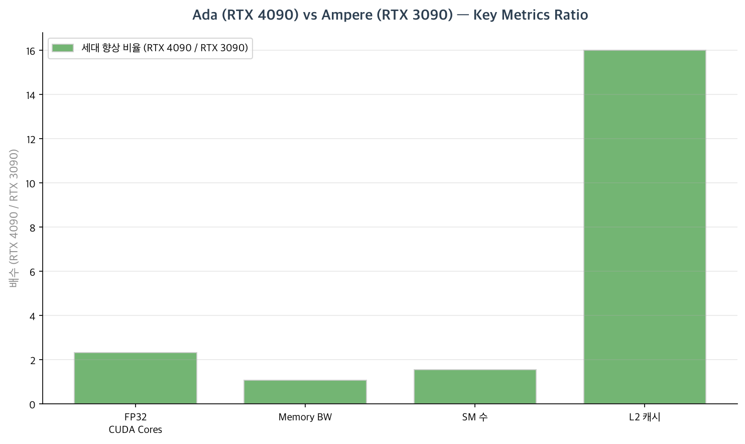
Memory bandwidth increased only 8%, while L2 cache grew 16×. The design philosophy: keep more working data on-chip rather than adding raw DRAM bandwidth.
3rd-Gen RT Cores
Throughput
The 3rd-gen RT Core delivers higher BVH intersection throughput per clock than the 2nd-gen Ampere counterpart. Two new dedicated acceleration engines accompany the throughput increase.
Opacity Micromap Engine (OME)
Problem: every alpha-textured triangle intersection invokes an AnyHit shader on the SM.
Leaves, chain-link fences, and particle effects use alpha transparency. Under the traditional RT pipeline, whenever a ray intersects such a triangle the RT Core must pause and invoke an AnyHit shader — running on an SM — to determine whether the intersection is accepted. This creates a round-trip stall on the RT Core.
OME solution: subdivide each triangle into micro-triangles and encode their opacity as 2 bits per micro-triangle, embedded directly in the BVH alongside geometry.
Micro-triangle opacity states:
  00 = Opaque      — ray hits unconditionally
  01 = Transparent — ray passes through (skip immediately)
  10 = Unknown     — invoke AnyHit shader
The RT Core reads these 2 bits during traversal and acts immediately:
Opaque: confirm intersection, no shader invocation neededTransparent: skip, continue traversalUnknown: fall back to AnyHit shader on the SM
Without OME:                            With OME:
Ray → triangle intersection             Ray → micro-triangle intersection
  → AnyHit shader (SM round-trip)         → Opaque: confirm immediately
  → opacity decision                       → Transparent: skip immediately
  → confirm or skip                        → Unknown: AnyHit only when needed
OME eliminates the SM round-trip for the common cases, dramatically increasing RT Core utilization in scenes with dense transparent geometry. The tradeoff is additional VRAM for the opacity micromap data alongside the BVH.
Displaced Micro-Mesh Engine (DMME)
Problem: high-detail surfaces require millions of triangles and correspondingly large BVHs.
Rock surfaces, terrain, and character skin require fine geometric detail for convincing ray tracing intersections. Representing that detail requires large triangle counts, which bloat the BVH and increase both traversal time and VRAM usage.
DMME solution: represent detailed surfaces as a low-polygon base mesh plus a compact displacement map. The RT Core evaluates ray-micro-triangle intersections procedurally during traversal, computing the displaced geometry on the fly.
Without DMME: base mesh (low poly)
              + tessellation → millions of triangles
              → large BVH → high VRAM usage

With DMME:   base mesh (low poly)
             + displacement map (compact)
             → RT Core evaluates displaced micro-geometry per intersection
             → smaller BVH → lower VRAM usage
Shader Execution Reordering (SER)
SER is Ada’s primary hardware-software co-optimization for ray tracing performance.
Problem: warp divergence from heterogeneous material hits.
In rasterization, neighboring pixels typically share the same triangle and material, so threads within a warp execute the same shader code. In ray tracing, each ray follows a unique BVH path and hits surfaces with different materials. When 32 threads in a warp each require a different ClosestHit shader, the GPU must serialize the executions — effectively running the 32 threads one shader type at a time.
SER solution: the GPU hardware buffers ClosestHit invocations in a queue and reorders them by shader type before dispatch, grouping threads with the same shader together.
Without SER:
Warp threads each hit different materials:
  Thread 0 → NatureShader   Thread 16 → GlassShader
  Thread 1 → RockShader     Thread 17 → NatureShader
  Thread 2 → GlassShader    ...
→ Each shader type serialized within the warp

With SER:
All intersection results queued as HitObjects
→ Sorted by shader type
NatureShader × N intersections → full warps → no divergence
RockShader   × M intersections → full warps → no divergence
GlassShader  × K intersections → full warps → no divergence
In DXR 1.2 (DirectX Raytracing), SER is accessed through the HitObject API. Shaders capture intersection results as HitObject values without immediately invoking the ClosestHit shader, then call ReorderThread() to let the hardware rearrange threads. After reordering, threads in the same warp share the same shader type, and HitObject::Invoke() executes with full coherence.
NVIDIA reported up to 2× improvement in shader throughput for complex ray tracing scenes.
4th-Gen Tensor Cores and FP8
Ada’s 4th-gen Tensor Cores are the same generation as Hopper’s. They support FP8 (E4M3, E5M2) inputs with FP32 accumulation. The FP8 format detail and Transformer Engine mechanics are covered in the Hopper post.
From Ada’s perspective, the key fact is that FP8 Tensor Core computation is available on a consumer GPU for the first time. Hopper brought FP8 to datacenter training; Ada brings the same Tensor Core generation to consumer inference workloads.
2:4 structured sparsity (introduced in Ampere) continues to be supported.
| Precision | RTX 3090 (GA102) | RTX 4090 (AD102) |
|---|---|---|
| FP32 CUDA Core | 35.6 TFLOPS | 82.6 TFLOPS |
| GDDR6X bandwidth | 936 GB/s | 1,008 GB/s |
| FP8 TC (Dense) | Not supported | Supported |
| FP16 TC (Sparse) | Supported | Supported |
Ada SM Structure
The Ada SM uses the same 4-sub-core structure as GA102. Changes are limited to TC and RT Core generations.
Ada SM (AD102, CC 8.9)
┌──────────────────────────────────────────────────────┐
│  Sub-core 0                  Sub-core 1              │
│  Warp Scheduler × 1          Warp Scheduler × 1      │
│  Dispatch Unit × 2           Dispatch Unit × 2       │
│  FP32 × 16 + FP32/INT32 × 16  (32 FP32 per sub-core)│
│  Tensor Core × 1 (4th gen)   Tensor Core × 1         │
│  LD/ST × 8 | SFU × 4        LD/ST × 8 | SFU × 4    │
├──────────────────────────────────────────────────────┤
│  Sub-core 2                  Sub-core 3              │
│  (identical structure)        (identical structure)   │
├──────────────────────────────────────────────────────┤
│  RT Core × 1 (3rd gen, shared across the SM)         │
├──────────────────────────────────────────────────────┤
│  L1 Cache + Shared Memory   128KB (configurable)     │
│  Register File              256KB                    │
└──────────────────────────────────────────────────────┘

Per-SM totals:
  FP32: 128 | INT32: 64 (dual-mode units)
  TC: 4 (4th gen — FP8/FP16/BF16/TF32/INT8)
  RT Core: 1 (3rd gen — OME + DMME capable)
  LD/ST: 32 | SFU: 16
GA102 vs AD102 SM comparison:
| GA102 (CC 8.6) | AD102 (CC 8.9) | |
|---|---|---|
| FP32 / SM | 128 | 128 |
| INT32 / SM | 64 | 64 |
| TC generation / SM | 3rd | 4th |
| RT Core generation / SM | 2nd | 3rd |
| LD/ST / SM | 32 | 32 |
| SFU / SM | 16 | 16 |
| L1 + Shared / SM | 128KB | 128KB |
| Register File / SM | 256KB | 256KB |
| Max Warps / SM | 48 | 48 |
| Max Blocks / SM | 16 | 24 |
The maximum resident blocks per SM increased from 16 to 24. Kernels with small block sizes benefit from higher occupancy — more blocks can co-reside on the same SM simultaneously.
96MB L2 Cache
GA102 had 6MB of L2. AD102 has 96MB — a 16× increase.
Why 96MB?
BVH traversal in ray tracing is fundamentally non-uniform. Each ray takes a unique path through the BVH structure, so spatial locality is poor and cache hit rates are low even with good scene design. The upper layers of a BVH (root and first few levels) are accessed by almost every ray, but 6MB was too small to keep even those nodes resident.
With 96MB, a complex scene’s BVH upper hierarchy can remain in L2 across an entire frame. The RT Core can retrieve upper-level nodes from L2 on every ray without triggering DRAM reads.
For inference workloads, 96MB accommodates larger activation and KV-cache slices for small-to-medium models, reducing DRAM traffic even without HBM.
GA102 (6MB L2):   BVH upper nodes evicted frequently → GDDR6X reads per ray
AD102 (96MB L2):  BVH upper nodes stay resident → L2 hits across rays
This explains why RTX 4090 delivers substantially higher ray tracing performance than RTX 3090 despite only 8% more memory bandwidth.
AD102’s L2 is physically partitioned across the die, but the cache coherency protocol presents it as a single 96MB unified space to software.
DLSS 3 and Frame Generation
DLSS 2.x (available since Turing) uses a Tensor Core–driven neural network to upscale frames from a lower render resolution — Super Resolution. Ada’s DLSS 3 adds Frame Generation on top.
Frame Generation mechanism:
DLSS 3 Frame Generation Pipeline

Rendered Frame N ────────────────────────────────┐
                                                  │
Rendered Frame N+1 ──────────────────────────── ─┤── AI network
                                                  │   (Tensor Cores)
Game engine motion vectors ─────────────────────── │     → Generated Frame G
                                                  │
Optical Flow Accelerator (5th-gen OFA) ───────────┘
  : computes dense per-pixel optical flow

Display output sequence: N → G → N+1 → G' → N+2 → ...
                          (one AI-generated frame inserted between each rendered pair)
Frame Generation is layered on top of DLSS Super Resolution: SR upscales each rendered frame to the target resolution, then Frame Generation inserts an AI-synthesized intermediate frame between every pair of SR-upscaled frames, approximately doubling the displayed frame count.
The 5th-gen Optical Flow Accelerator (OFA) is the enabling hardware. OFA has been present since Turing, but Ada’s 5th-gen version has sufficient throughput for real-time frame generation. RTX 30-series cards cannot support Frame Generation through a software update — the hardware generation gap is fundamental.
Frame Generation adds a small amount of input latency because the AI-generated frame is inserted after rendering completes. NVIDIA Reflex mitigates this by reducing the render queue depth between the game engine and the driver, recovering most of the added latency.
Scheduling
Ada’s warp scheduling model carries forward from Ampere. Each SM has 4 independent warp schedulers issuing instructions every clock. Independent Thread Scheduling (per-thread program counter, introduced in Volta) is retained.
CC 8.9 occupancy limits:
| GA102 (CC 8.6) | AD102 (CC 8.9) | |
|---|---|---|
| Max warps / SM | 48 | 48 |
| Max blocks / SM | 16 | 24 |
| Max threads / SM | 1,536 | 1,536 |
Maximum warps per SM is unchanged; the increase from 16 to 24 maximum blocks per SM allows more co-resident blocks when using smaller block sizes, improving occupancy for kernels with 64 or 32 threads per block.
SER operates at the hardware-software interface level, not within the SM warp scheduler itself. The SM schedulers are structurally unchanged; SER is a separate buffering and sorting engine that acts before shader invocation.
Interconnect and External Channels
PCIe Host Interface
| Architecture | PCIe | Note |
|---|---|---|
| Ada Lovelace (AD102) | 4.0 x16 | Same as Ampere |
| Hopper (GH100) | 5.0 x16 | First PCIe 5.0 |
| Ampere (GA102) | 4.0 x16 | First PCIe 4.0 |
Ada retained PCIe 4.0. The PCIe 5.0 transition was exclusive to Hopper in this generation.
NVLink
Consumer RTX 40-series GPUs have no NVLink. RTX 30-series (GA102) included an NVLink bridge connector for peer-to-peer; Ada removed it entirely. Ada-based professional cards (L40, L40S) also lack NVLink and use PCIe for host connectivity.
L2 Cache and Memory Subsystem
| Product | L2 Cache | DRAM | Bus Width | Bandwidth |
|---|---|---|---|---|
| RTX 3090 (GA102) | 6MB | GDDR6X | 384-bit | 936 GB/s |
| RTX 4090 (AD102) | 96MB | GDDR6X | 384-bit | 1,008 GB/s |
| RTX 4080 (AD103) | 64MB | GDDR6X | 256-bit | 717 GB/s |
| RTX 4070 Ti (AD104) | 48MB | GDDR6X | 192-bit | 504 GB/s |
L2 cache scales down proportionally across the die family, not just die area.
NVENC / NVDEC
| RTX 3090 (GA102) | RTX 4090 (AD102) | L40S (AD102) | |
|---|---|---|---|
| NVENC count | 1 | 2 (dual) | 2 (dual) |
| AV1 encode | Yes | Yes | Yes |
| H.264 / HEVC encode | Yes | Yes | Yes |
| AV1 decode | Yes | Yes | Yes |
AD102 and AD103 carry dual NVENC — the first consumer GPUs with two independent video encoders. This enables simultaneous streaming and local recording at full quality, or two independent encode streams. Dies AD104 and smaller (RTX 4070 Ti and below) carry a single NVENC.
Display Outputs (consumer reference)
| Product | DisplayPort | HDMI | Max Resolution |
|---|---|---|---|
| RTX 4090 (AD102) | 1.4a × 3 | 2.1 × 1 | 7,680×4,320 (with DSC) |
| RTX 4080 (AD103) | 1.4a × 3 | 2.1 × 1 | 7,680×4,320 (with DSC) |
| L40S (AD102, professional) | None | None | — |
L40S is a datacenter inference card — no display outputs.
Summary
| GA102 (Ampere) | AD102 (Ada) | |
|---|---|---|
| Process | Samsung 8nm | TSMC 4N |
| Transistors | 28.3B | 76.3B |
| FP32 throughput | 35.6 TFLOPS | 82.6 TFLOPS |
| TC generation | 3rd | 4th (FP8) |
| RT Core generation | 2nd | 3rd (OME, DMME) |
| SER | None | Yes |
| L2 Cache | 6MB | 96MB |
| Memory bandwidth | 936 GB/s | 1,008 GB/s |
| Register File / SM | 256KB | 256KB |
| Max Warps / SM | 48 | 48 |
| Max Blocks / SM | 16 | 24 |
| PCIe | 4.0 x16 | 4.0 x16 |
| NVLink | 3.0 (RTX 3090) | None |
| NVENC count (AD102) | 1 | 2 (dual) |
| Frame Generation | None | DLSS 3 |
Ada Lovelace more than doubled compute throughput from Ampere while structurally addressing the main ray tracing bottlenecks. The 96MB L2 keeps BVH upper-layer nodes resident across a frame. OME eliminates SM round-trips for transparent geometry. SER recovers warp utilization from divergent material hits. Together these changes compound: the raw RT Core throughput gain understates the real-world rendering improvement.
The next post covers Blackwell — FP4 Tensor Cores, MXFP8 microscaling, and the two-die MCM architecture.
References
- NVIDIA. NVIDIA Ada Lovelace GPU Architecture Technical Brief. 2022.
- NVIDIA. DLSS 3 Technical Overview. NVIDIA Developer Blog, 2022.
- NVIDIA. Shader Execution Reordering: Bringing Order to Chaos with Hardware-Accelerated Ray Tracing. NVIDIA Developer Blog, 2022.
- NVIDIA. GeForce RTX 4090 Product Specifications. NVIDIA.com.
- NVIDIA. CUDA C++ Programming Guide, Appendix H: Compute Capabilities. CUDA Toolkit Documentation.